
Parasitic Capacitance
Interactive Audio Lesson
Listen to a student-teacher conversation explaining the topic in a relatable way.
Introduction to Parasitic Capacitance
🔒 Unlock Audio Lesson
Sign up and enroll to listen to this audio lesson

Today, we're discussing parasitic capacitance, which refers to the unintended capacitance that arises between conductive elements at high frequencies. Can anyone tell me why this is particularly significant in RF and HF circuits?

It's because the size of the components becomes comparable to the wavelength of the signals.
Exactly! As frequency increases, spatial dimensions start to play a role. Parasitic capacitance can significantly affect our circuit's performance. What are some examples you think might exhibit these effects?

I think PCB traces and component leads would have parasitic capacitance.
You're correct! PCB traces interacting with ground planes or other traces create capacitance, and leads between components also contribute to this phenomenon. Let's remember it with the acronym 'P-CAP' for Parasitic CAPacitance as a helpful memory aid!
Effects of Parasitic Capacitance
🔒 Unlock Audio Lesson
Sign up and enroll to listen to this audio lesson

Now that we've defined parasitic capacitance, let's discuss its effects. How do you think it alters the frequency response of a circuit?

I think it can make the circuit respond suddenly or lag because of changes in capacitance.
Exactly, it can distort the desired frequency response, leading to potential inefficiencies. Furthermore, what do we call the issue when signals unintentionally transfer due to parasitic capacitance?

That's called crosstalk.
Right! Crosstalk can result in unwanted interference in signals. To avoid this, we need careful design consideration. A good rule of thumb to remember is 'design away crosstalk'.
Design Considerations for High-Frequency Circuits
🔒 Unlock Audio Lesson
Sign up and enroll to listen to this audio lesson
So, what are some strategies we can implement to mitigate the effects of parasitic capacitance while designing high-frequency circuits?
We should keep signal traces short and well-spaced.
Good point! By minimizing trace lengths and keeping them apart, we can reduce parasitic effects. Can anyone think of any other techniques?
Using ground planes effectively might help too, right?
Absolutely! Ground planes can help shield and provide a stable reference, ultimately reducing unwanted capacitance. Remember, 'Space is Grace' to reflect on designing with distance in mind!
Summary of Key Takeaways
🔒 Unlock Audio Lesson
Sign up and enroll to listen to this audio lesson
Let’s summarize what we’ve covered about parasitic capacitance. Can anyone give me a definition?
It's the unintended capacitance that arises between conductive elements due to electric fields.
Perfect! And what impacts does it have on circuit performance, especially related to frequency response?
It can alter the circuit's response and create crosstalk, leading to interference.
Exactly! And what design strategies help mitigate these issues?
Keeping traces short, well-spaced, and using ground planes effectively!
Well done, everyone! Remember, by understanding parasitic capacitance, we can improve our designs and reduce unwanted effects.
Introduction & Overview
Read summaries of the section's main ideas at different levels of detail.
Quick Overview
Standard
In high-frequency circuits, parasitic capacitance emerges due to the proximity of conductors, particularly in PCB traces and component leads. This phenomenon alters frequency response and can lead to crosstalk, necessitating careful design considerations in high-frequency applications.
Detailed
Detailed Summary on Parasitic Capacitance
Parasitic capacitance is a critical factor in high-frequency circuit design, primarily arising from unintended capacitance between conductive elements. At radio frequencies (RF) and high frequencies (HF), all conductors inherently exhibit parasitic capacitance due to electric field interactions between them. Notably, this capacitance is significant in two main areas:
- PCB Traces: The capacitance can occur between signal traces and ground planes or between different signal traces, influencing the circuit's frequency response.
- Component Leads: The capacitance between leads of components such as resistors, capacitors, and inductors also plays a role in altering circuit behaviors.
The effects of parasitic capacitance include:
- Alteration of Frequency Response: Changes in capacitance directly influence how a circuit responds to high-frequency signals, potentially leading to performance degradation.
- Unintended Coupling: Parasitic capacitance enables crosstalk—a critical issue where signals unintentionally transfer between components or traces, resulting in interference.
Understanding parasitic capacitance and its impacts is vital in optimizing high-frequency circuit performance, as neglecting these effects can lead to inefficiencies and signal integrity issues.
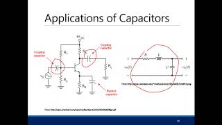
Youtube Videos

Audio Book
Dive deep into the subject with an immersive audiobook experience.
Presence of Parasitic Capacitance at High Frequencies
Chapter 1 of 2
🔒 Unlock Audio Chapter
Sign up and enroll to access the full audio experience
Chapter Content
At high frequencies, all conductors exhibit parasitic capacitance due to the electric fields between them. This capacitance is especially significant in:
● PCB traces: The capacitance between signal traces and the ground plane or between different signal traces.
● Component leads: The capacitance between the leads of components like resistors, capacitors, and inductors.
Detailed Explanation
At high frequencies, every conductor in a circuit acts like it has an additional capacitor connected to it. This is because electric fields develop between conductors, leading to an effect known as parasitic capacitance.
- PCB Traces: When we look at PCB (Printed Circuit Board) traces, these are the little paths that carry electrical signals. They can unintentionally gather electrical charge, especially when they run close to a ground plane or when they are close to other signal traces. This is because the electric field creates capacitance.
- Component Leads: Similarly, the leads (or wires) connecting components like resistors and capacitors can also create capacitive effects when they are close together. This is important as it can affect how the circuit operates at high frequencies.
Examples & Analogies
Think of parasitic capacitance like the 'echo' effect when you shout in a large empty room. Just like your voice can bounce off the walls, electrical signals can 'bounce' between conductors, creating unintended signals. For example, if you shout (send a strong signal) while other people are in the room (other traces or components), they might hear your echo (the parasitic capacitance's effect) affecting their conversation (the expected output of the circuit).
Impact on Circuit Performance
Chapter 2 of 2
🔒 Unlock Audio Chapter
Sign up and enroll to access the full audio experience
Chapter Content
Parasitic capacitance can:
● Alter the frequency response of the circuit, especially at high frequencies.
● Create unintended coupling between components, leading to crosstalk.
Detailed Explanation
When parasitic capacitance is present in a circuit, it leads to several problems:
- Frequency Response Changes: As the frequency of signals increases, the influence of parasitic capacitance means that the circuit does not behave as expected. This can cause certain frequencies to be amplified more or less than intended.
- Crosstalk: This is when signals from one part of the circuit affect signals in another part. The unintended coupling can lead to noise or interference, compromising the integrity of the signals.
Examples & Analogies
Imagine you're at a party where several conversations are happening around you. If one person starts to talk loudly (a signal), it can distract others or even make it hard to hear your own conversation (signal integrity). Similarly, in a circuit, if one trace (line carrying the signal) develops parasitic capacitance and begins to pick up too much signal from its neighbor, it leads to confusion (crosstalk). This is why in circuit design, engineers work hard to minimize these effects to keep the conversations clear.
Key Concepts
-
Parasitic Capacitance: Unintended capacitance due to electrical field interactions in high-frequency circuits.
-
Frequency Response: Changes in circuit behavior at different frequencies due to capacitance.
-
Crosstalk: Unwanted signal interference stemming from parasitic capacitance.
Examples & Applications
In a PCB design, overlapping traces may introduce parasitic capacitance, affecting the integrity of high-speed signals.
Capacitance between the leads of a capacitor in a circuit can result in unintended coupling, altering circuit behavior.
Memory Aids
Interactive tools to help you remember key concepts
Rhymes
In high frequencies, capacitance grows, causing signals to misbehave and idle flows.
Stories
Imagine a crowded room where everyone is shouting—no one hears their own voice. This is what happens due to crosstalk from parasitic capacitance in circuits!
Memory Tools
C-R-A-F-T: Capacitance, Response, Alteration, Frequency, Transfer.
Acronyms
P-CAP
Parasitic CAPacitance exemplifies the issue at hand.
Flash Cards
Glossary
- Parasitic Capacitance
Unintended capacitance that occurs between conductive elements, affecting circuit performance.
- Crosstalk
Unwanted transfer of signals between communication circuits, due to parasitic capacitance or inductance.
- PCB Traces
Conductive pathways on printed circuit boards that connect different components.
Reference links
Supplementary resources to enhance your learning experience.