
Parasitic Effects in High-Frequency Circuits
Interactive Audio Lesson
Listen to a student-teacher conversation explaining the topic in a relatable way.
Parasitic Capacitance
🔒 Unlock Audio Lesson
Sign up and enroll to listen to this audio lesson

Today, let's discuss parasitic capacitance, which occurs due to the electric fields between conductors. How do you think this affects circuit design at high frequencies?

I suppose it could change how signals behave, right?
Exactly! It can alter the frequency response and create unwanted component interaction called crosstalk. Parasitic capacitance is significant in PCB traces, where it affects signal integrity.

What kind of issues does crosstalk cause?
Crosstalk leads to interference between signals, which can corrupt data. Remember the acronym CTC: Crosstalk, Timing, and Coupling—these are critical aspects to keep in mind.

Could designing traces with more space help?
Great thought! Increasing the distance helps minimize parasitic capacitance, thereby reducing crosstalk.
To summarize, parasitic capacitance can significantly affect circuit performance by altering responses and inducing crosstalk.
Parasitic Inductance
🔒 Unlock Audio Lesson
Sign up and enroll to listen to this audio lesson

Moving on to parasitic inductance, can anyone tell me where you might encounter this in a circuit?

On the component leads or PCB traces, right?
Yes! Parasitic inductance can delay signals and affect integrity. A mnemonic to remember this is 'LIE', meaning Leads Increase Effects.
How do long traces specifically impact it?
Long traces can increase inductance, leading to voltage drops and altered impedance. This highlights the necessity of short, direct routes in designs.
Does this apply to all frequencies, or is it more pronounced at higher ones?
It's indeed more pronounced at higher frequencies. The rapid changes in current exacerbate the effects of parasitic inductance.
To wrap up, parasitic inductance can significantly compromise signal integrity, especially in fast-switching circuits.
Skin Effect
🔒 Unlock Audio Lesson
Sign up and enroll to listen to this audio lesson
Next, let's address the skin effect. Who can explain what this is in the context of AC?
Isn’t it when AC tends to flow near the surface of a conductor?
Exactly! This effect increases the resistance of the conductor as frequency rises. Can someone tell me how this impacts circuit performance?
It can make circuits less efficient, right? More resistance means more power loss?
Correct! The skin effect leads to higher effective resistance, particularly significant in RF and microwave circuits. A simple analogy is a crowded swimming pool—more swimmers only use the edges, not the center.
So, using thicker conductors can help reduce the impact?
Yes! Wider conductors can alleviate some of the effects as they provide more surface area. In summary, skin effect increases resistance with frequency and challenges efficient design.
Stray Coupling and Crosstalk
🔒 Unlock Audio Lesson
Sign up and enroll to listen to this audio lesson
Lastly, let’s delve into stray coupling and crosstalk. Can anyone explain what they are?
Stray coupling refers to unintended signal transfer between components?
Exactly! Crosstalk is a result of this coupling. It can occur through capacitive or inductive means, especially in closely spaced traces. Remember the ‘SCC’: Stray Coupling Causes interference.
What can we do to minimize this?
Maintaining distance between traces, using shielding techniques, and proper grounding are essential strategies.
Can we measure this interference somehow?
Absolutely! Tools like oscilloscopes can help visualize and quantify crosstalk effects in a circuit. In summary, being aware of stray coupling and implementing design strategies is crucial for signal integrity.
Introduction & Overview
Read summaries of the section's main ideas at different levels of detail.
Quick Overview
Standard
As circuit frequencies increase, parasitic effects become increasingly significant in high-frequency circuit design. This section covers parasitic capacitance, inductance, skin effect, and crosstalk, all of which can adversely affect circuit performance and signal integrity.
Detailed
Detailed Summary of Parasitic Effects in High-Frequency Circuits
As the frequency of operation elevates, parasitic effects—unwanted capacitance and inductance—must be taken into account when designing circuits. This section delves into four primary aspects of parasitic effects:
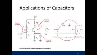
- Parasitic Capacitance: Found between conductors, especially on PCB traces and component leads, this can modify frequency responses and lead to crosstalk.
- Parasitic Inductance: Manifested in all conductors, it can cause signal integrity issues and delay, particularly with long leads and traces.
- Skin Effect: This behavior of AC tends to cause current to flow near the surface of conductors, increasing resistance and losses at high frequencies.
- Stray Coupling and Crosstalk: This includes capacitive and inductive coupling that can inadvertently transfer signals, causing interference and noise. Understanding these effects is crucial for maintaining signal integrity and effective circuit performance.
Youtube Videos


Audio Book
Dive deep into the subject with an immersive audiobook experience.
Introduction to Parasitic Effects
Chapter 1 of 5
🔒 Unlock Audio Chapter
Sign up and enroll to access the full audio experience
Chapter Content
As the frequency increases, parasitic effects become more pronounced and must be considered in high-frequency circuit design. These parasitics arise from the physical layout of components, leads, and interconnections.
Detailed Explanation
Parasitic effects refer to the unwanted electrical characteristics that arise due to the physical layout and proximity of components in a circuit. As the operating frequency of circuits increases, these effects can significantly impact performance. Every electronic component and wire has some inherent capacitance, inductance, and resistance that can influence circuit behavior. For example, the way components are arranged on a printed circuit board (PCB) can create unintended paths for current, altering the intended operation of the circuit. Hence, high-frequency circuit designers must account for these parasitic effects to avoid issues like signal integrity degradation and performance bottlenecks.
Examples & Analogies
Think of parasitic effects like traffic on a busy road where unexpected detours (parasitics) can divert cars (signals) away from their destination. If a road is not well planned and cars (signals) are rerouted unexpectedly, it can lead to congestion (signal distortion), delays, and inefficiencies in reaching the intended endpoint (circuit performance).
Parasitic Capacitance
Chapter 2 of 5
🔒 Unlock Audio Chapter
Sign up and enroll to access the full audio experience
Chapter Content
At high frequencies, all conductors exhibit parasitic capacitance due to the electric fields between them. This capacitance is especially significant in:
● PCB traces: The capacitance between signal traces and the ground plane or between different signal traces.
● Component leads: The capacitance between the leads of components like resistors, capacitors, and inductors.
Parasitic capacitance can:
● Alter the frequency response of the circuit, especially at high frequencies.
● Create unintended coupling between components, leading to crosstalk.
Detailed Explanation
Parasitic capacitance occurs when two conductive parts are close enough that they influence each other through electric fields. In high-frequency circuits, such as those found in RF applications, these capacitances can significantly affect how signals behave. For example, the tiny spaces between conductive traces on a PCB can introduce unwanted capacitance that alters how the circuit responds to different frequencies. This could cause signals to blend or interfere with each other, known as crosstalk, potentially leading to erroneous circuit behavior. Additionally, the overall frequency response of a circuit may be modified, which can hinder circuit functionality.
Examples & Analogies
Imagine you are at a party where multiple conversations are happening at once. If you are too close to another conversation, you might overhear parts of it (crosstalk). Similarly, when components in a circuit are too close together, their unintended electric interactions can distort the signals they are meant to transmit or receive.
Parasitic Inductance
Chapter 3 of 5
🔒 Unlock Audio Chapter
Sign up and enroll to access the full audio experience
Chapter Content
All conductors, including PCB traces and component leads, exhibit parasitic inductance. At high frequencies, these inductances affect the signal's behavior, particularly in circuits with fast switching or high-frequency signals.
● Inductance of leads: Long leads or traces can introduce significant inductance, affecting the signal integrity and causing delays.
● Trace inductance: The inductance of PCB traces can lead to voltage drops and changes in the impedance of the circuit.
Detailed Explanation
Parasitic inductance is another unwanted effect caused by the arrangement of conductors in a circuit. It manifests when a conductor's length increases and can lead to significant issues, such as delays in signal transmission and alterations in circuit impedance. Inductance tends to store energy in its magnetic field when current flows through it, which can also mean that the signal experiences lag, leading to timing issues, especially in fast-switching applications. Moreover, the longer the trace or lead, the higher the parasitic inductance, thus designers aim to keep leads short to minimize this effect.
Examples & Analogies
Consider a long rubber band being pulled: the longer it is, the more it can stretch before it provides resistance to motion. Similarly, longer electrical traces can introduce more inductance, causing signals to 'stretch' or delay when traveling through the circuit, hampering their performance.
Skin Effect
Chapter 4 of 5
🔒 Unlock Audio Chapter
Sign up and enroll to access the full audio experience
Chapter Content
The skin effect is the tendency of alternating current (AC) to flow near the surface of a conductor at high frequencies. This effect increases the effective resistance of the conductor and reduces the available cross-sectional area for current flow, leading to increased losses.
● High-frequency resistance: The resistance of conductors increases with frequency due to the skin effect, which impacts the performance of RF circuits, especially at microwave frequencies.
Detailed Explanation
The skin effect occurs in conductive materials when alternating currents are applied, causing the current to distribute unevenly across the conductor's cross-section. Instead of flowing uniformly through the entire area, AC tends to flow along the 'skin' or surface. This phenomenon results in an increase in effective resistance at high frequencies, leading to greater energy losses in the form of heat. For RF designers, understanding and mitigating the skin effect is vital because it can severely diminish circuit efficiency and increase operational costs.
Examples & Analogies
Think of the skin effect like squeezing a tube of toothpaste. When you squeeze the tube (apply AC), the toothpaste (current) comes out mostly from the edges of the tube (surface), rather than evenly from the whole tube. As a result, if the tube were much larger than necessary, you might have wasted toothpaste that is not being efficiently utilized - similar to how high-frequency signals can suffer from inefficiency due to the skin effect!
Stray Coupling and Crosstalk
Chapter 5 of 5
🔒 Unlock Audio Chapter
Sign up and enroll to access the full audio experience
Chapter Content
At high frequencies, stray coupling can occur between circuit traces, components, or wires, leading to crosstalk. Crosstalk refers to the unintended transfer of signals from one circuit to another, which can cause interference and noise.
● Capacitive coupling: Occurs when signals are unintentionally coupled through parasitic capacitance.
● Inductive coupling: Occurs when signals are coupled through parasitic inductance, often seen in closely spaced PCB traces.
Detailed Explanation
Stray coupling happens when electromagnetic fields from one circuit unintentionally influence others nearby, leading to crosstalk. This can occur through capacitive or inductive coupling depending on how the components are arranged. Capacitive coupling occurs when two adjacent conductors share electric fields, while inductive coupling happens when the magnetic fields resulting from changing currents influence each other. Both of these coupling mechanisms can introduce noise and degrade the performance of circuits, causing them to behave unpredictably. Therefore, careful design and layout practices are essential to minimize these interactions.
Examples & Analogies
Picture two people sharing a close workspace: if one person speaks loudly (generating a strong signal), the other may overhear (crosstalk) parts of that conversation. Similarly, in circuits, if components or traces are too close without adequate shielding or separation, they can unintentionally share information, leading to interference.
Key Concepts
-
Parasitic Capacitance: Unintentional capacitance that can alter frequency responses.
-
Parasitic Inductance: Unwanted inductance causing delays in high-frequency signals.
-
Skin Effect: Increased resistance in conductors due to AC current concentrating near surfaces.
-
Crosstalk: Interference between signals from unwanted coupling.
-
Stray Coupling: Unintended coupling of signals leading to interference.
Examples & Applications
An example of parasitic capacitance can be seen in PCB designs where traces run parallel to one another, creating capacitance that can lead to cross-interference.
Parasitic inductance becomes particularly problematic in high-speed digital circuits where long leads on components can cause delays that affect timing and synchronization.
Memory Aids
Interactive tools to help you remember key concepts
Rhymes
Capacitance and inductance show, in circuits high, they tend to grow.
Stories
Imagine a crowded pool where swimmers only use the edges to avoid bumping into each other—that's how the skin effect limits current flow in a conductor.
Memory Tools
S.C.C. - Stray Coupling Causes interference, helps in remembering the impact of stray effects.
Acronyms
C.T.C. for Crosstalk, Timing, and Coupling, helps recall key areas of concern in high-frequency design.
Flash Cards
Glossary
- Parasitic Capacitance
Capacitance that occurs unintentionally between conductors which can alter frequency responses and create crosstalk.
- Parasitic Inductance
Inductance that results from the physical characteristics of conductors, which can affect signal integrity and cause delays.
- Skin Effect
The phenomenon where alternating current tends to flow near the surface of a conductor, increasing effective resistance at high frequencies.
- Crosstalk
Unintended transfer of signals between circuits or conductors, resulting in interference.
- Stray Coupling
Unintended coupling of signals due to proximity between circuit elements, leading to interference.
Reference links
Supplementary resources to enhance your learning experience.