
Practical Applications of Distributed Effects
Interactive Audio Lesson
Listen to a student-teacher conversation explaining the topic in a relatable way.
High-Frequency Signal Transmission
🔒 Unlock Audio Lesson
Sign up and enroll to listen to this audio lesson

Today, we're discussing how distributed effects affect high-frequency signal transmission. Can anyone tell me why this is important?

Because signals can get distorted if the effects aren't considered?
Exactly! When we deal with high frequencies, like in microwave communications, the components' sizes become significant relative to the signal's wavelength. This means that the way signals travel can change drastically.

So, how does that impact something like an antenna?
Great question! Antennas are designed to transmit or receive signals effectively. If we ignore distributed effects, we risk poor performance, such as signal loss or interference.
PCB Layout Design
🔒 Unlock Audio Lesson
Sign up and enroll to listen to this audio lesson

Moving onto PCB layout design—can someone explain what the main focus should be here?

Routing signal traces properly?
Exactly! Proper routing reduces parasitic capacitance and inductance. This is critical for maintaining signal integrity, especially at high frequencies. You have to ensure your ground planes are well designed as well.

Does component placement also matter?
Absolutely! Good component placement can minimize unwanted coupling between circuits. Think of it like giving each component enough space to ‘breathe’!
Signal Integrity
🔒 Unlock Audio Lesson
Sign up and enroll to listen to this audio lesson
Now let's discuss signal integrity. Why is this critical in high-frequency circuits?
Because it helps prevent errors in data transmission?
That's right! To achieve signal integrity, we need to understand and manage distributed effects and parasitic losses throughout the circuit.
So is impedance matching always important?
Yes! Proper impedance matching minimizes reflections, ensuring that the signal flows smoothly through the entire system, which is vital for high-speed data applications.
Real-World Applications
🔒 Unlock Audio Lesson
Sign up and enroll to listen to this audio lesson
Can anyone think of a specific application where these principles might apply?
What about GPS technology? It uses high-frequency signals.
Absolutely! GPS systems must ensure high signal integrity to provide accurate location information. Distributed effects can severely disrupt communications in these systems.
What about satellite communications?
That's another excellent example! In satellite communications, managing these distributed effects is crucial due to the long distances signals must travel.
Introduction & Overview
Read summaries of the section's main ideas at different levels of detail.
Quick Overview
Standard
In Section 5.5, the practical applications of distributed effects are explored in the context of high-frequency circuits. Key applications include their impact on signal transmission, PCB layout design, and maintaining signal integrity. Proper management of these effects is crucial for optimizing performance in systems such as antenna designs and microwave communications.
Detailed
Practical Applications of Distributed Effects
In high-frequency circuit design, understanding distributed effects is essential for several real-world applications. Distributed effects play a crucial role in:
- High-Frequency Signal Transmission: These effects are particularly significant in systems such as antenna designs, high-speed data transmission, and microwave communication systems. As signals travel through these systems, their performance can be heavily influenced by how well distributed effects are managed, ensuring efficient signal propagation.
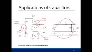
- PCB Layout Design: Careful PCB layout is vital in mitigating parasitic effects. This includes the routing of signal traces and proper grounding to uphold signal integrity at high frequencies. The placement of components can help reduce interference caused by distributed capacitance and inductance.
- Signal Integrity: In contemporary communication systems, maintaining high signal integrity is paramount. This requires a thorough understanding of the inherently distributed nature of RF and HF circuits, which encompasses minimizing losses due to parasitic effects and ensuring proper impedance matching across circuits to enhance performance.
By applying these principles in practical scenarios, engineers can optimize circuit designs for high-frequency applications, leading to significant improvements in performance and reliability.
Youtube Videos

Audio Book
Dive deep into the subject with an immersive audiobook experience.
High-Frequency Signal Transmission
Chapter 1 of 3
🔒 Unlock Audio Chapter
Sign up and enroll to access the full audio experience
Chapter Content
Distributed effects are significant in systems such as antenna designs, high-speed data transmission, and microwave communication systems.
Detailed Explanation
High-frequency signal transmission involves the use of antennas and communication systems that operate at radio frequencies (RF) or higher. At these frequencies, the physical characteristics of the circuit and its components influence how signals are transmitted, causing distributed effects to play a major role. The behavior of the electromagnetic fields and their distribution can change how signals propagate, potentially causing delays or losses if not properly managed.
Examples & Analogies
Think of a high-frequency signal like a wave moving through water. If the water is smooth, the wave travels efficiently. However, if there are obstacles (like rocks), the wave can be disrupted. In high-frequency systems, components act similarly to those rocks at the ocean’s surface — they can interfere with signal transmission. This is why engineers must carefully design antennas to ensure signals reach their destination without unnecessary interference.
PCB Layout Design
Chapter 2 of 3
🔒 Unlock Audio Chapter
Sign up and enroll to access the full audio experience
Chapter Content
Careful routing of signal traces, component placement, and proper grounding are critical to managing parasitic effects and ensuring signal integrity at high frequencies.
Detailed Explanation
Printed Circuit Board (PCB) layout is crucial for the performance of high-frequency circuits. The way components are placed, how traces are routed, and how grounding is managed can mitigate issues caused by parasitic capacitance and inductance. Poor layout leads to unwanted coupling between traces and affects the overall integrity of the signal. Engineers must optimize these elements to ensure that signals remain strong and clear as they traverse the circuit.
Examples & Analogies
Imagine organizing a busy street with cars representing signals. If the street (the PCB) has clear signs (properly placed components and traces), the traffic flows smoothly. But if street signs are confusing or if cars are parked poorly (poor component layout), traffic jams (signal degradation) occur. A well-designed PCB ensures that every signal can flow freely to its destination without interference.
Signal Integrity
Chapter 3 of 3
🔒 Unlock Audio Chapter
Sign up and enroll to access the full audio experience
Chapter Content
In modern communication systems, ensuring high signal integrity requires understanding the distributed nature of RF and HF circuits. This includes minimizing losses due to parasitics and ensuring the proper impedance matching across the entire system.
Detailed Explanation
Signal integrity is about maintaining the quality of the electrical signal as it travels through a circuit. At high frequencies, even small losses or mismatches can lead to significant problems like reflections and crosstalk. Understanding distributed effects helps engineers design systems that minimize these losses. Achieving proper impedance matching ensures that signals can flow efficiently without being reflected back, which maintains the integrity and clarity of the communication.
Examples & Analogies
Consider a long, fast-moving train as a signal. If the tracks are well-aligned with no gaps (proper impedance matching), the train can travel smoothly. However, if there are bumps or gaps (mismatched impedance), the train can wobble or even derail (loss of signal integrity). By ensuring everything is aligned and continuous, we keep the train, or signal, on the right track.
Key Concepts
-
High-Frequency Signal Transmission: Important in antenna design, data transmission, and communication systems, where signal propagation is critical.
-
PCB Layout Design: Significant factors include routing signal traces and component placements to minimize parasitic effects.
-
Signal Integrity: Essential for ensuring accurate and reliable communication, requires careful handling of distributed effects and impedance matching.
Examples & Applications
GPS technology requires high fidelity in signal integrity due to the reliance on high-frequency signals which are sensitive to distributed effects.
Satellite communications systems must manage distributed effects diligently to maintain signal quality over large distances.
Memory Aids
Interactive tools to help you remember key concepts
Rhymes
In high-frequency land, watch out for the wave,
Stories
Imagine a race where the cars (signals) need clear roads (traces). If the roads are bumpy (parasitics), the cars won’t finish smoothly (signal integrity).
Memory Tools
For high-frequency design, remember 'Get Signal Perfect' (GSP): Group signals, Shield traces, Protect connections.
Acronyms
PCBS - PCB Considerations
Placement
Clearance
Grounding
Signaling.
Flash Cards
Glossary
- HighFrequency Signal Transmission
The process of transmitting signals at frequencies high enough that distributed effects become significant.
- PCB Layout Design
The process of designing printed circuit boards while considering the placement, routing, and proper grounding of components.
- Signal Integrity
The ability of a signal to maintain its integrity during transmission, minimally affected by noise, distortion, and loss.
- Parasitic Effects
Unwanted effects in electrical circuits that arise from the physical properties of components and layout, particularly at high frequencies.
- Impedance Matching
The process of ensuring that the impedance of a load matches the impedance of the transmission line to maximize power transfer.
Reference links
Supplementary resources to enhance your learning experience.