
Analog Electronic Circuits
Enroll to start learning
You’ve not yet enrolled in this course. Please enroll for free to listen to audio lessons, classroom podcasts and take practice test.
Interactive Audio Lesson
Listen to a student-teacher conversation explaining the topic in a relatable way.
Voltage Gain Analysis
🔒 Unlock Audio Lesson
Sign up and enroll to listen to this audio lesson

Today, we will analyze the voltage gain of the Common Collector amplifier and how the introduction of additional resistances, like R_L, affects it.

What happens if R_L is not very high? Will that change our calculations?
Excellent question! If R_L is not very high, we'll need to adjust our calculations as it comes into play with r_o, effectively changing the voltage gain formula.

Can you remind us what the original voltage gain formula was?
Sure! The original voltage gain formula assumes an ideal scenario without additional resistances and can be expressed as A_v = r_o/(r_o + R_L).

Will this formula still hold true when we include practical resistances?
Yes, but we must be careful to substitute r_o with the effective value considering R_L. This means A_v will be less than ideal but we can approximate it under certain conditions.

Got it! So, lower R_L means lower voltage gain, right?
Exactly! That's a critical takeaway. Remember, voltage gain close to unity is a key feature in Common Collector amplifiers, especially in buffering applications.
To summarize, we learned that the introduction of practical resistances affects the voltage gain significantly, and we should always analyze those effects in circuit design.
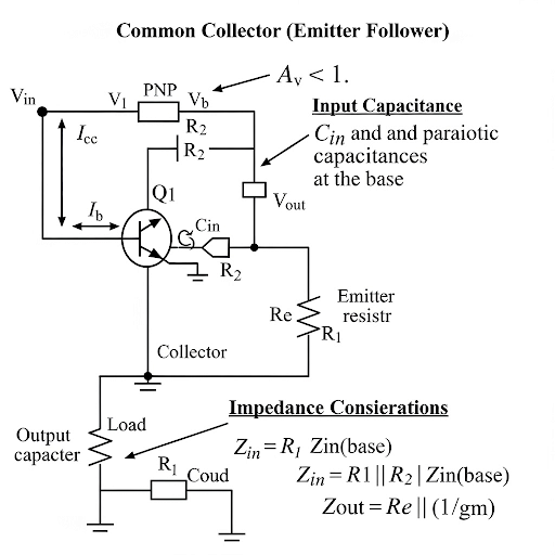
Input Capacitance
🔒 Unlock Audio Lesson
Sign up and enroll to listen to this audio lesson

Next, let's consider input capacitance. How do you think parasitic capacitance affects our circuit?
I assume it would introduce more complexity to the overall capacitance?
That's correct! The input capacitance could be expressed as C_in = C_µ + C_π(1 - A_v).
What role does the voltage gain play here?
If A_v approaches unity, the impact of C_π will be minimized. Hence, input capacitance is vital in determining the circuit's frequency response.
How should we account for C_gd and C_gs in our analysis?
These capacitances represent gate-to-drain and gate-to-source effects in MOSFETs. They will also need to be considered in calculating overall input capacitance.
So, we should design with these parameters in mind to avoid unwanted frequency limitations.
Absolutely! Always remember – input capacitance can shape the behavior of your amplifier across frequency ranges.
To recap, input capacitance including parasitic effects can significantly alter circuit behavior, especially in high-frequency applications.
Impedance Considerations
🔒 Unlock Audio Lesson
Sign up and enroll to listen to this audio lesson
Now let's shift to output impedance. Why is it essential for us to know the output resistance of the common collector amplifier?
I think it determines how well the amplifier can drive loads, right?
Exactly! The output resistance can impact how well the amplifier functions when connected to varying loads.
What factors affect output resistance?
Good question! We've discussed resistances in parallel and the dominance of g_m in practical scenarios that can change this value.
So, we can use this knowledge to optimize our circuit designs?
Absolutely! A buffer amplifier should ideally have low output impedance to effectively isolate the preceding stages.
And how does varying R_L affect this?
If R_L is significantly lower, it will dominate, making the output resistance more prominent. Always check the balance of resistances during design.
In summary, output impedance is crucial for load driving capability and should be accounted for in all designs.
Introduction & Overview
Read summaries of the section's main ideas at different levels of detail.
Quick Overview
Standard
In this section, we delve deeper into the analysis of Common Collector and Common Drain Amplifiers, considering realistic circuit components to evaluate voltage gain, impedance, input capacitance, and output resistance. The emphasis is on understanding how practical elements affect these parameters compared to ideal models.
Detailed
In this section, we continue the exploration of Common Collector (CC) and Common Drain (CD) amplifiers, building upon previous discussions of their basic principles and ideal characteristics. The focus now shifts to incorporating real-world circuit components and understanding their practical implications on the performance of these amplifiers.
Key Topics Covered
- Voltage Gain Analysis: We begin by analyzing the voltage gain of the Common Collector amplifier with the introduction of additional resistances such as R_L. By recognizing the effect of these resistances, we refine our understanding of feedback mechanisms that influence the gain.
- Input Capacitance: We also explore input capacitance in the context of practical components including parasitic capacitances. The comprehensive formula for input capacitance takes into consideration various circuit elements and their interactions.
- Impedance Considerations: The impedance of the amplifiers is re-evaluated, focusing on how including resistive loads changes the output resistance. The section discusses examples and calculations that help in grasping how these resistances impact overall performance.
-
Practical Significance: The theoretical aspects discussed serve to illustrate how real-world scenarios and component tolerances lead to variations in expected amplifier behavior. The analysis culminates in the reiteration of design principles for effective amplifier circuits.
This section is crucial for students of electronics to build a robust foundation in amplifier design by bridging theoretical knowledge with practical applications.
Youtube Videos

Audio Book
Dive deep into the subject with an immersive audiobook experience.
Introduction to Common Collector and Common Drain Amplifiers
Chapter 1 of 7
🔒 Unlock Audio Chapter
Sign up and enroll to access the full audio experience
Chapter Content
Dear students, welcome back to our online NPTEL certification course. The topic of this course is Analog Electronic Circuit. Myself, Pradeep Mandal from E and ECE department of IIT Kharagpur. Today’s topic of discussion it is Common Collector and Common Drain Amplifiers, rather I should say it is continuation of this topic.
Detailed Explanation
In this introduction, Professor Pradip Mandal welcomes the students back to the course and recaps the focus on Analog Electronic Circuits, specifically common collector and common drain amplifiers. This sets the stage for a continuation of the previous discussions, emphasizing the practical aspects of these amplifiers and their components.
Examples & Analogies
Think of this course like a cooking class where each session builds on the last. Just like how each recipe might use ingredients from the previous ones, today’s lesson will use concepts we already covered about amplifiers and add more practical details.
Overview of Today's Topics
Chapter 2 of 7
🔒 Unlock Audio Chapter
Sign up and enroll to access the full audio experience
Chapter Content
So, what we have to cover today, as I said we have discussed the motivation part of the common source and sorry common collector and common drain amplifier, basic operation and biasing also it is done. And we are going to go a little detail of analysis of voltage gain and impedance, input capacitance, considering realistic biasing and their associated components.
Detailed Explanation
In this chunk, the professor outlines the topics for the day's lecture, which include a more in-depth analysis of common collector and common drain amplifiers. Topics include voltage gain, impedance, and input capacitance while taking realistic components into account. This provides a clear roadmap for what students can expect to learn.
Examples & Analogies
Just like a construction project where the blueprint gives a detailed plan, this outline helps students understand what to expect in the session. If you were building an amplifier, you'd want to know about its strength (gain), foundations (impedance), and size (capacitance) before calling it complete.
Common Collector Amplifier Analysis
Chapter 3 of 7
🔒 Unlock Audio Chapter
Sign up and enroll to access the full audio experience
Chapter Content
So, to start with let we let you consider the common collector amplifier and also in the common collector amplifier we are including this R . So, this R may be coming from the bias circuit...
Detailed Explanation
This section begins with an analysis of the common collector amplifier, emphasizing the inclusion of a load resistance (R). The professor explains the significance of considering this resistance in the amplifier's analysis to better understand its practical implications. It highlights the transition from theoretical concepts to real-world applications.
Examples & Analogies
Imagine you've built a bridge. The load resistance is like the weight of vehicles using the bridge. While designing it, considering the weight ensures the bridge will be stable and safe under real usage conditions.
Small Signal Equivalent Circuit
Chapter 4 of 7
🔒 Unlock Audio Chapter
Sign up and enroll to access the full audio experience
Chapter Content
we do have small signal equivalent circuit of the common collector amplifier having this R included. So, we do have r here and then g v , r coming from the MOS at the BJT transistor...
Detailed Explanation
Here, the professor discusses the small signal equivalent circuit of the common collector amplifier. This model allows for a simplified analysis of the amplifier's performance under small signal conditions by representing active components with their small signal parameters. The inclusion of specific resistances and transistor parameters is crucial for accurate calculations.
Examples & Analogies
Think of a small signal equivalent circuit like a miniature model of a complex machine. Just like a model can help you understand how the actual machine works, this simplified version helps us analyze the bigger circuit's behavior in real conditions.
Impact of Practical Components on Voltage Gain
Chapter 5 of 7
🔒 Unlock Audio Chapter
Sign up and enroll to access the full audio experience
Chapter Content
Now, if we have this R which is essentially coming in parallel with r then whatever the derivation we have done before that can be as well utilized just by replacing this r by r and R in parallel.
Detailed Explanation
In examining the impact of resistances on voltage gain, the professor explains how the parallel arrangement of the load resistance (R) and the internal resistance (r) changes the voltage gain calculation. This adjustment reflects the real-world scenario where these resistances affect how the amplifier performs.
Examples & Analogies
Consider trying to pour water through two size openings (resistances). If one is wider (lower resistance) than the other, the flow (gain) is increased. In practical circuits, all these openings must be accounted for to understand the overall flow of electrical signals.
Input Capacitance Analysis
Chapter 6 of 7
🔒 Unlock Audio Chapter
Sign up and enroll to access the full audio experience
Chapter Content
Likewise, when you consider the input capacitance if you see the expression or if you recall the previous expression of the input resistance without considering this R , what we had it is...
Detailed Explanation
The professor delves into the concept of input capacitance, emphasizing how its calculation changes when the load resistance is included. He reiterates how previous theoretical formulations must be updated to consider practical components, enhancing students' understanding of circuit behavior.
Examples & Analogies
Imagine trying to fill a balloon (input capacitance) with different types of liquids (currents). The thickness of the liquid will impact how quickly you can fill it (the capacitance behavior). Understanding how changes in components affect this filling process helps predict the performance of the circuit.
Output Resistance Considerations
Chapter 7 of 7
🔒 Unlock Audio Chapter
Sign up and enroll to access the full audio experience
Chapter Content
So, if you see this circuit and at this point if you see what is the output resistance, it is basically the output resistance coming from the rest of the circuit coming in parallel with R .
Detailed Explanation
This chunk focuses on output resistance in the common collector amplifier. The professor explains how output resistance is calculated based on the parallel configuration of various resistances in the circuit. Understanding output resistance is vital for assessing how the amplifier interacts with subsequent stages in a circuit.
Examples & Analogies
Think of output resistance like a team of athletes running a relay. If some athletes (resistances) are faster (lower resistance), the team’s overall performance will improve. Similarly, in circuits, proper analysis of output resistance ensures that the heart of the circuit can pass signals effectively.
Key Concepts
-
Common Collector Amplifier: Provides high input and low output impedance, ideal for matching circuits.
-
Voltage Gain: Key characteristic that indicates the amplification factor, typically close to 1 in CC amplifiers.
-
Input Capacitance: Influences the frequency response of amplifiers, including parasitic effects.
-
Output Impedance: A critical factor in determining an amplifier's capability to drive loads effectively.
Examples & Applications
Using a Common Collector amplifier in audio equipment to buffer signals by maintaining unity voltage gain.
Incorporating input capacitance considerations in high-speed circuit designs to ensure minimal signal degradation.
Memory Aids
Interactive tools to help you remember key concepts
Rhymes
In a CC amp where signals fly, input high, output low, oh me, oh my!
Stories
Imagine a bridge (Common Collector) that lets electric signals travel easily from one side (input) to the other (output) without dropping luggage (voltage gain).
Memory Tools
Remember 'VIGOR': Voltage, Input gain, Gain close to one, Output resistance low, Resistance influences output.
Acronyms
CIPC
Common Collector
Input Capacitance
Practical components
Combine those ideas!
Flash Cards
Glossary
- Common Collector Amplifier
An amplifier configuration that provides high input impedance and low output impedance.
- Voltage Gain
Ratio of output voltage to input voltage; indicates how much an amplifier increases signal strength.
- Input Capacitance
The capacitance seen at the input terminal of an amplifier, affected by parasitic elements.
- Output Impedance
The equivalent resistance seen by the load at the output terminal of an amplifier.
- R_L
The load resistance connected to the output of an amplifier, significant in determining voltage gain.
Reference links
Supplementary resources to enhance your learning experience.