
Common Drain Stage Analysis
Enroll to start learning
You’ve not yet enrolled in this course. Please enroll for free to listen to audio lessons, classroom podcasts and take practice test.
Interactive Audio Lesson
Listen to a student-teacher conversation explaining the topic in a relatable way.
Basic Operation and Structure
🔒 Unlock Audio Lesson
Sign up and enroll to listen to this audio lesson

Today, we will explore the common-drain amplifier, commonly known as a source follower. This configuration is crucial for buffer applications, whereby we can achieve a high input impedance and a low output impedance.

Why do we call it a source follower?
Great question! It follows the input signal at the source terminal, meaning whatever voltage comes in at the gate will appear at the source with slight modifications based on gain factors.

So, does that mean it has a voltage gain close to 1?
Exactly! The voltage gain is approximately equal to 1, especially when output load resistance is significantly higher than the intrinsic output resistance.

Can we write that as an equation?
Yes! We can express it as A_v ≈ 1 - (R_L/(R_L + r_ds)). It’s important to understand how the addition of various resistances can influence gain.
Voltage Gain Analysis
🔒 Unlock Audio Lesson
Sign up and enroll to listen to this audio lesson

Now, let’s analyze the voltage gain in detail. The presence of load resistance alters our gain slightly.

How does it impact the overall performance?
When R_L is introduced in parallel with the output resistance r_ds, the gain decreases marginally. However, in many practical circuits, this can be negligible.
What happens if the load resistance is very small?
If R_L is small, it will significantly pull down the gain because the voltage division across R_L will come into play. Always consider your total circuit conditions when designing!
Input Capacitance Considerations
🔒 Unlock Audio Lesson
Sign up and enroll to listen to this audio lesson
Input capacitance in our circuit arises from gate-source capacitance and gate-drain capacitance.
What equations do we use to define that?
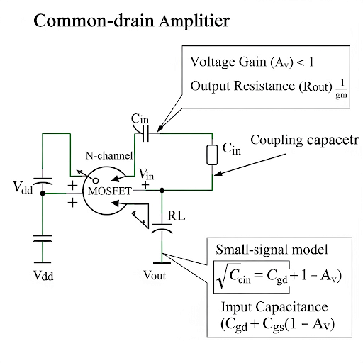
The total input capacitance, C_in, is given by C_gs plus C_gd altered by the voltage gain: C_in = C_gs + C_gd(1 - A_v).
In practical terms, how does this affect signal integrity?
Since C_gs tends to present a high capacitive effect, its size directly skews input behavior affecting bandwidth and transient responses.
Output Resistance and Practical Considerations
🔒 Unlock Audio Lesson
Sign up and enroll to listen to this audio lesson
Finally, let's focus on the output resistance which dictates how the common-drain amplifier interfaces with subsequent stages.
So how do we derive this theoretically?
By analyzing the currents flowing through and the conductances at play, we can conclude R_out is mainly determined by g_m.
Why is this important to know?
Output resistance affects the ability of the amplifier to drive loads; a low output resistance is crucial for an effective buffer stage.
Introduction & Overview
Read summaries of the section's main ideas at different levels of detail.
Quick Overview
Standard
In this section, we explore the workings of common-drain amplifiers by analyzing their voltage gain, input capacitance, and output resistance. Key components and their contributions to circuit performance are discussed, namely, the effects of realistic biasing and resistances on amplifier characteristics.
Detailed
Common Drain Stage Analysis
This section provides a detailed examination of common-drain amplifiers, also known as source followers. The analysis includes the parameters of voltage gain, output resistance, and input capacitance, emphasizing the impact of practical circuit components on these values.
1. Basic Operation and Structure
The common-drain amplifier configuration includes essential parameters such as the device transconductance and resistances from the biasing circuits.
2. Voltage Gain Analysis
The voltage gain for a common-drain amplifier was explored, building on previous analyses while considering the influence of a load resistance (R_L) in parallel with the intrinsic output resistance (r_ds). The impact on gain is expressed as:
\[ A_v \approx 1 - \frac{R_L}{R_L + r_{ds}} \]
This indicates that the voltage gain approximates unity under ideal conditions, but the inclusion of R_L modifies it slightly.
3. Input Capacitance
The formulas for input capacitance depend on gate-source capacitance (C_gs) and gate-drain capacitance (C_gd). The total input capacitance takes into account the voltage gain effect, leading us to derive that C_in remains relatively small in practical applications.
4. Resistance Analysis:
The output resistance derived is typically dominated by transconductance (g_m) and less influenced by load resistances, maintaining the characteristics needed for buffering operations. The significant takeaway here is the resistance remains reasonably low depending on various factors such as the R_L and feedback conditions.
Through this analysis, we conclude that the essence of the common-drain amplifier lies in its ability to provide stability and gain close to 1, while balancing the interactions with various resistors in practical circuits.
Youtube Videos

Audio Book
Dive deep into the subject with an immersive audiobook experience.
Introduction to Common Drain Amplifiers
Chapter 1 of 4
🔒 Unlock Audio Chapter
Sign up and enroll to access the full audio experience
Chapter Content
The common drain stage considering R and its voltage gain, voltage gain it is given here. So, again you may recall the previous analysis where we have not considered R, for that the voltage gain it was ...
Detailed Explanation
The common drain amplifier is one type of transistor amplifier that is configured to provide a certain voltage gain. When analyzing its performance, we begin with a simplified model that does not consider additional resistances initially. In previous discussions, the voltage gain was established without considering R. However, when this resistance is included, it comes into play mainly with respect to the output impedance and modifies the gain slightly as it introduces additional factors that must be taken into account.
Examples & Analogies
Think of a common drain amplifier like a water pipe system. Initially, we measure how much water flows through without any restrictions (R). When we add a valve (R), although it might slightly affect the water flow, the flow remains largely unaffected if the valve is wide open. Only when we start closing the valve does it impact the overall flow significantly.
Voltage Gain Analysis
Chapter 2 of 4
🔒 Unlock Audio Chapter
Sign up and enroll to access the full audio experience
Chapter Content
Now, in presence of this R this R it is coming in parallel with r. So, you may say that wherever we do have the r, we can we can replace this r by r ⫽ R and that gives us the corresponding voltage gain.
Detailed Explanation
In the analysis of the common drain amplifier's voltage gain, when we include the resistance R, it impacts the calculation of the overall gain. Specifically, R is combined with the internal resistance 'r', which leads to a new expression for voltage gain. By parallelly analyzing these resistances, we can derive a modified expression that accounts for both components. This is crucial because it allows us to understand how these elements interact and influence the performance of the circuit.
Examples & Analogies
Imagine calculating the total speed of two cars running parallel to each other on a freeway. If one car (the internal resistance r) is going 70 mph, and you add another lane (the external resistance R), the combined effect on traffic speed would depend on how both lanes contribute together. By merging these speeds into a combined metric, we can better understand the overall flow of traffic.
Capacitance and Input Resistance
Chapter 3 of 4
🔒 Unlock Audio Chapter
Sign up and enroll to access the full audio experience
Chapter Content
Likewise, when you consider the input capacitance if you see the expression or if you recall the previous expression of the input resistance without considering this R, what we had it is ...
Detailed Explanation
Input capacitance refers to the way that the amplifier's input responds to changing signals. Previously, we derived the input resistance without including R. Now, with the inclusion of R, it is evident that it modifies our input resistance and capacitance calculations. This is important, as these parameters influence how quickly the amplifier can react to input signals and how it affects the overall performance.
Examples & Analogies
Consider how a sponge (amplifier) absorbs water (input signal). If the sponge has a hole (input resistance), it can soak up faster. However, if you close that hole slightly by adding a cover (R), the sponge's ability to absorb water is affected, even though it can still function. The effect of R is analogous to modifying that hole on the sponge—changing the parameters of absorption but not completely stopping it.
Output Resistance Considerations
Chapter 4 of 4
🔒 Unlock Audio Chapter
Sign up and enroll to access the full audio experience
Chapter Content
If you see this circuit and at this point if you see what is the output resistance, it is basically the output resistance coming from the rest of the circuit coming in parallel with R.
Detailed Explanation
The output resistance of the common drain amplifier is a key parameter because it influences how the amplifier interacts with the load it drives. By analyzing the output resistance, we recognize that it results from the remaining circuitry's resistance combined with R. The parallel configuration often leads to a lower effective output resistance, enhancing the amplifier's ability to drive loads.
Examples & Analogies
Imagine a group of friends trying to lift a heavy object. If one friend (the load) is strong, they can lift it alone. However, if another friend (R) helps, the overall effort is shared. In this way, the total weight lifted (output resistance) is less than the weight of the individual friends alone. They work together to reduce the strain on any single individual in the group.
Key Concepts
-
Voltage Gain: The step around voltage output to input ratios, near 1 in ideal scenarios.
-
Input Capacitance: Total capacitance impacting signal integrity; derived from gate-source and gate-drain capacitances.
-
Output Resistance: Affects the interfacing ability of an amplifier; critical for ensuring minimal load disturbance.
Examples & Applications
Example 1: If an amplifier has a load resistance of 10kΩ and an intrinsic output resistance of 2kΩ, the voltage gain reduces to A_v ≈ 0.833.
Example 2: A common-drain amplifier with C_gs of 15nF and a voltage gain of 1 results in an input capacitance of 15nF, while if A_v is reduced, C_in may increase due to the gate-drain capacitance.
Memory Aids
Interactive tools to help you remember key concepts
Rhymes
Common-drain to buffer is the game, keeping signal integrity, that’s its claim.
Stories
Imagine a water pipe—the source is the input flow, maintaining pressure as it flows down into a bucket—the output—where water collects without much loss; the design keeps everything steady!
Memory Tools
GIV (Gain, Input, Voltage) is how we remember the three core aspects of analyzing common-drain stages.
Acronyms
CROSS (Common Drain, Resistance, Output, Source, Signals) encapsulates essential components we need to review.
Flash Cards
Glossary
- CommonDrain Amplifier
An amplifier configuration that provides input impedance high and output impedance low, often used for buffering applications.
- Voltage Gain (A_v)
The ratio between output voltage to input voltage, commonly expressed in decibels (dB).
- Output Resistance (R_out)
The resistance seen looking into the output terminal of the circuit; influences how the circuit interacts with load.
- Input Capacitance (C_in)
The net capacitance at the input terminal, affecting frequency response and signal integrity.
- Transconductance (g_m)
A measure of the change in output current for a change in input voltage, indicating the amplifier's gain factor.
- Load Resistance (R_L)
The resistance connected to the output of an amplifier, impacting its voltage gain.
- GateSource Capacitance (C_gs)
Capacitance between the gate and source terminals in a field-effect transistor.
Reference links
Supplementary resources to enhance your learning experience.