
Common Collector Amplifier Analysis
Enroll to start learning
You’ve not yet enrolled in this course. Please enroll for free to listen to audio lessons, classroom podcasts and take practice test.
Interactive Audio Lesson
Listen to a student-teacher conversation explaining the topic in a relatable way.
Understanding Voltage Gain in Common Collector Amplifiers
🔒 Unlock Audio Lesson
Sign up and enroll to listen to this audio lesson

Today, let's start with the basic voltage gain of the common collector amplifier. Can anyone remind me what we discussed about its ideal voltage gain?

The voltage gain is approximately equal to 1, isn’t it?
Correct! This means the output voltage closely follows the input voltage. Now, how might this change when we include load resistance (R_L)?

Doesn’t it slightly lower the gain due to changes in the output impedance?
Exactly! Loading effects can have a significant impact, but we often approximate elements for simplicity. Let’s remember the acronym A = 1 for our typical outcomes. How about we revisit this to ensure full understanding?

Could you explain how the load resistance affects the voltage gain?
Great question! Load resistance parallels with output resistance, so we need to account for that. If we denote r_o as the output resistance, then voltage gain A can be defined by its modified resistance.

Can you summarize the key points about voltage gain?
Sure! The voltage gain is ideally 1, but may be affected by load resistance. Remember to think about output resistance and how it parallels with load resistance.
Exploring Input and Output Impedance
🔒 Unlock Audio Lesson
Sign up and enroll to listen to this audio lesson

Now, let's delve into input and output impedance. Why is it critical to maintain high input impedance in amplifiers?
It prevents loading down the previous circuit stage, right?
Precisely! It preserves signal integrity. In addition to that, how do we calculate output impedance in the presence of load resistance?
We would still consider the parallel combination of resistances.
Right again! Remember that the output impedance approaches close to 0 in practical terms, which is an essential characteristic. Does anyone remember how we denote this relationship?
Isn’t it through the reciprocal of total conductance?
That’s correct! So, output impedance relates to the combination of all conductances in parallel. To recap, high input impedance prevents loading, and output impedance closely interacts with load resistance.
Impact of Practical Components
🔒 Unlock Audio Lesson
Sign up and enroll to listen to this audio lesson
Next, let’s consider how practical components like capacitance affect performance. What key elements can we identify?
We should take capacitors such as C_μ and C_π into account, right?
Absolutely! They significantly impact the input capacitance and should be considered in a realistic scenario. How does this interaction affect our voltage gain?
I think the capacitance interacts with voltage gain, making it lower than 1?
Very good thought! It can lead to frequency-dependent behavior, impacting overall performance. We will note that for input capacitance, C_total = C_μ + C_π(1-A).
Could you summarize the effects of practical components?
Certainly! Practical components like parasitic capacitances reduce voltage gain and affect input capacitance, reminding us of the importance of realistic circuit design.
Consideration of Source Resistance
🔒 Unlock Audio Lesson
Sign up and enroll to listen to this audio lesson
Now, let’s discuss source resistance and its role. Why is it considered in the common collector amplifier?
It could change the input voltage seen by the amplifier!
Exactly! Considering the voltage divider effect is crucial. How do we generally approach the analysis?
We simplify our analysis by assuming high R_s compared to input resistance.
Correct! Hence, the base voltage is slightly lower, but this doesn’t affect gain significantly if R_s is large. Remember this voting strategy for input-output voltage relation, especially in practical designs.
What's the key takeaway in considering source resistance?
Good question! It's vital to understand how it interacts with the amplifier's input characteristics. Although important, its impact remains limited provided R_s is high enough.
Resistance within Common Collector Amplifier
🔒 Unlock Audio Lesson
Sign up and enroll to listen to this audio lesson
Finally, let’s analyze the resistance connected to the collector terminal. Why is it important in our circuit design?
It provides a path for output and could change the behavior of our amplifier!
Exactly! While primary input and output terminals remain unchanged, the presence of resistance alters output characteristics. How do we adapt our calculations?
We treat it like other components but monitor its impact closely?
Great insight! When assessing output and voltage characteristics, we validate how additions impact voltage gain calculations. Recap, it’s all about monitoring those connections.
Can you summarize the roles of additional capacitances or resistances?
Certainly! Additional components can enrich our understanding of circuit performance, allowing us to optimize design by observing gains adjusted by resistances at the collector. Key formulas remain the same, but attention is crucial!
Introduction & Overview
Read summaries of the section's main ideas at different levels of detail.
Quick Overview
Standard
In this section, we examine the common collector amplifier's performance by analyzing its voltage gain, input capacitance, and output resistance, incorporating realistic circuit elements. The implications of various resistances within the amplifier are discussed to elucidate the amplifier's behavior in practical applications.
Detailed
Common Collector Amplifier Analysis
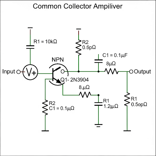
The common collector amplifier, often referred to as an emitter follower, acts as a voltage buffer with significant implications in circuit design. This section delves into the detailed analysis of its operational characteristics, including:
- Voltage Gain: The voltage gain (A) is essential to consider under both ideal and practical scenarios. The equation derived (A ≈ 1) holds true even when accounting for additional load resistance (R_L) parallel to the output resistance (r_o).
- Impedance: The input impedance (R_in) remains high, ensuring minimal loading effect on preceding stages. The analysis reveals that even when including load resistance, the input resistances add up significantly without major alterations to the original design characteristics.
- Capacitance Effects: Various capacitive elements (C_μ and C_π) affect the input capacitance in real-world scenarios. The relationship between input capacitance and voltage gain highlights the importance of maintaining minimal capacitance for optimal performance.
-
Practical Component Impact: The section explains scenarios where practical components, such as biasing resistors and source resistance, affect the amplifier's behavior without significantly altering its basic function.
These analyses underscore the practical significance of common collector amplifiers in design applications, confirming their efficacy as voltage followers while considering realistic variances in circuit components.
Youtube Videos

Audio Book
Dive deep into the subject with an immersive audiobook experience.
Introduction to Common Collector Amplifier Analysis
Chapter 1 of 9
🔒 Unlock Audio Chapter
Sign up and enroll to access the full audio experience
Chapter Content
Dear students, welcome back to our online NPTEL certification course. The topic of this course is Analog Electronic Circuit. Myself, Pradeep Mandal from E and ECE department of IIT Kharagpur. Today’s topic of discussion it is Common Collector and Common Drain Amplifiers, rather I should say it is continuation of this topic. Previous day we have discussed about relatively idealistic bias situation and today we are going to a little detail considering some practical circuit components also.
Detailed Explanation
In this introductory section, the instructor sets the stage for the analysis of common collector amplifiers by referencing previous lectures. He emphasizes that today's discussion will build upon earlier concepts and delve into more practical aspects of circuit components.
Examples & Analogies
Think of this as a classroom where students learned the basics of cooking before. Now, the teacher is taking them to a kitchen to apply those basic cooking skills using real ingredients and tools, enhancing their knowledge with practical experience.
Analysis Focus Areas
Chapter 2 of 9
🔒 Unlock Audio Chapter
Sign up and enroll to access the full audio experience
Chapter Content
So, what we have to cover today, as I said we have discussed the motivation part of the common source and sorry common collector and common drain amplifier, basic operation and biasing also it is done. And we are going to go a little detail of analysis of voltage gain and impedance, input capacitance, considering realistic biasing and their associated components.
Detailed Explanation
The instructor outlines the key areas of focus for the analysis of the common collector amplifier. These include its voltage gain, impedance, and input capacitance, particularly when realistic biasing conditions are applied, contrasting this with the earlier ideal scenarios.
Examples & Analogies
Imagine studying the theory of driving a car in a classroom and now preparing to actually drive on the road. You need to understand the mechanics of how the car operates under realistic conditions, including adjustments based on varying traffic situations.
Circuit Analysis with Practical Components
Chapter 3 of 9
🔒 Unlock Audio Chapter
Sign up and enroll to access the full audio experience
Chapter Content
In fact, in the previous class we have discussed about the analysis of the circuit for voltage gain, impedance and input capacitance ignoring these components, and today we are going to see what will be there you know consequences if we consider on practical components. So, let us start with the common collector amplifier, considering the R_L, and then we will be moving to the next one is considering the source resistance R_S.
Detailed Explanation
This chunk highlights the transition from theoretical analysis to practical circuit considerations. The analysis looks at how introducing real-world components (like resistors) affects the voltage gain and input capacitance of the common collector amplifier. The instructor introduces two specific resistors that will be analyzed: R_L (load resistor) and R_S (source resistance).
Examples & Analogies
Just like adjusting the settings on a sound mixer to manage real audio recordings, understanding how each resistor impacts the signal ensures optimal performance of the amplifier in real-world scenarios.
Including Load Resistor R_L
Chapter 4 of 9
🔒 Unlock Audio Chapter
Sign up and enroll to access the full audio experience
Chapter Content
So, to start with let we let you consider the common collector amplifier and also in the common collector amplifier we are including this R_L. So, this R_L may be coming from the bias circuit, representing the finite conductance of the bias circuit or maybe and or maybe additional load resistance we are connecting at the output node with respect to ground.
Detailed Explanation
In this section, the focus shifts to R_L, which is a crucial part of the common collector amplifier circuit. The instructor explains that R_L can originate from various sources, including biasing circuits or load resistors connected to ground, affecting the overall circuit behavior.
Examples & Analogies
Thinking about this in terms of a water system, R_L can be compared to pipes of different diameters added to a water flow system; they influence how water flows through the pipes depending on their size and configuration.
Understanding Input Capacitance
Chapter 5 of 9
🔒 Unlock Audio Chapter
Sign up and enroll to access the full audio experience
Chapter Content
Now, in our previous analysis where we have excluded this R_L there we have seen the expression of the input capacitance. Basically, the input capacitance at the base with respect to the AC ground.
Detailed Explanation
Here, the instructor discusses the input capacitance of the amplifier, which is the capacitance observed at the base when considering the AC ground. The previous analyses did not factor in R_L, and now this component will be included to see how it influences the input capacitance.
Examples & Analogies
Consider this as a sponge being filled with water—without the sponge (R_L), the water (signal) can flow easily, but as you introduce sponges of different sizes (resistors), the water’s flow changes, simulating how input capacitance affects signal transmission.
Voltage Gain Changes with R_L
Chapter 6 of 9
🔒 Unlock Audio Chapter
Sign up and enroll to access the full audio experience
Chapter Content
So, if we put this expression of this voltage gain here, so this is A_v. So, if you put that voltage gain expression here, what we will be getting here it is C_in having C and then C part it is having a factor which is a having in the numerator we do have r and in the denominator we do have (R_L // r_o) + this r_pi.
Detailed Explanation
The focus now shifts to how the inclusion of R_L influences the voltage gain of the common collector amplifier. The expression reveals that the voltage gain A_v is dependent on the resistive elements in the circuit, showing how the presence of R_L alters the previous gain approximation.
Examples & Analogies
Think of this like adjusting the volume control on a speaker. As you adjust it, the sound level (voltage gain) changes based on the input source impacted by the environment (R_L), illustrating the dynamic nature of electronic signals.
Effects of Source Resistance R_S
Chapter 7 of 9
🔒 Unlock Audio Chapter
Sign up and enroll to access the full audio experience
Chapter Content
In fact, you can further simplify this one wherever we do have the you may replace this by β of the transistor. So, here also we can write this is (r_pi + R_L) = ... .
Detailed Explanation
This section discusses the impact of source resistance R_S on the input and output characteristics of the amplifier. By estimating the input resistance in the presence of R_S, the instructor highlights how simple substitutions (like using β) can streamline calculations.
Examples & Analogies
Imagine tuning a musical instrument where subtle adjustments make a significant effect on sound quality. Here, just a small resistance can change the output and input characteristics, much like the strings of an instrument impact its sound.
Output Resistance Factors
Chapter 8 of 9
🔒 Unlock Audio Chapter
Sign up and enroll to access the full audio experience
Chapter Content
Now, that is about the common collector amplifier if you consider its counterpart mass counterpart namely the common drain stage and then if you consider this R_L for that, what you will be getting it is similar kind of things we can get only difference is that this r_pi, it will not be there.
Detailed Explanation
In this part, the instructor compares common collector amplifiers to common drain stages, examining output resistance characteristics. It is concluded that while there are similarities, there are also distinct differences regarding specific parameters.
Examples & Analogies
It's similar to comparing two types of musical instruments. Both may play music, but the sound output (resistance) and the way they resonate (circuit behavior) can be quite different, showcasing their unique characteristics.
Practical Implications of R_S and R_L
Chapter 9 of 9
🔒 Unlock Audio Chapter
Sign up and enroll to access the full audio experience
Chapter Content
In conclusion, we have discussed various aspects of the common collector amplifier, including the effects of R_L and R_S on voltage gain, input capacitance, and output resistance.
Detailed Explanation
The instructor summarizes the detailed analysis of the common collector amplifier, reflecting on how the inclusion of resistors like R_L and R_S influences key parameters. This wrap-up reinforces the practical implications of these components in real circuit designs.
Examples & Analogies
Just as a writer revises their drafts considering feedback to improve the final story, engineers must also refine their circuit designs based on practical components, ensuring the final performance meets desired specifications.
Key Concepts
-
Common Collector Configuration: Provides high input impedance and low output impedance, maintaining voltage stabilities.
-
Voltage Gain Approximation: The gain is ideally close to 1 under typical operation.
-
Capacitive Influence: Parasitic capacitances impact input capacitance leading to reduced effective gain.
-
Practical Components: Real resistances/rms affect amplifier behavior but can often be simplified in calculations.
Examples & Applications
In practice, a common collector amplifier can serve in buffering applications, maintaining signal integrity in audio devices.
When designing a sensor interface, employing a common collector amplifier allows for high input impedance, ensuring accurate signal sampling without degradation.
Memory Aids
Interactive tools to help you remember key concepts
Rhymes
To follow a signal, make it your goal, use a common collector, it’s on a roll!
Stories
Imagine a relay race where the first runner passes the baton (signal) smoothly to the next, symbolizing the function of a common collector as a buffer, maintaining the momentum of the signal.
Memory Tools
G-A-I-N: Gain Approximation Is Near 1 for the common collector.
Acronyms
I-P-R
Input resistance is high
output is low
voltage gain is approximately 1.
Flash Cards
Glossary
- Common Collector Amplifier
An amplifier configuration where the output is taken from the emitter, providing voltage buffering with high input impedance.
- Voltage Gain
The ratio of output voltage to input voltage, indicating how much an amplifier increases the strength of a signal.
- Input Impedance
The impedance seen by the input signal, crucial for ensuring minimal loading effect on prior circuit stages.
- Output Impedance
The impedance at the output terminal of the amplifier, influencing how much voltage drops across the output when a load is connected.
- Capacitance Effects
The influence of capacitive components within the amplifier circuit, particularly with respect to input capacitance and frequency response.
Reference links
Supplementary resources to enhance your learning experience.