
Analog Electronic Circuits
Enroll to start learning
You’ve not yet enrolled in this course. Please enroll for free to listen to audio lessons, classroom podcasts and take practice test.
Interactive Audio Lesson
Listen to a student-teacher conversation explaining the topic in a relatable way.
Introduction to Common Collector and Common Drain Amplifiers
🔒 Unlock Audio Lesson
Sign up and enroll to listen to this audio lesson

Welcome class! Today we're diving into the concepts of common collector and common drain amplifiers. Can anyone tell me why we might want to use these configurations?

I think they're used to improve performance when cascading amplifiers?
Exactly! They help mitigate issues like voltage gain degradation. These amplifiers have high input impedance and low output impedance. Let's remember that with the mnemonic 'HIGH LOW' where H stands for High input and L for Low output impedance.

So, they are designed to prevent loading effects when we connect multiple stages?
Yes, perfect! These configurations act as buffers, isolating the stages. What do you think the voltage gain of these amplifiers is?

Is it close to 1?
Correct! The voltage gain is approximately 1, meaning minimal attenuation of the signal.

What about the input and output capacitances?
Good question! We aim for minimal input and output capacitances to improve frequency response. Always think in terms of performance metrics!
Detailed Analysis of Circuit Performance
🔒 Unlock Audio Lesson
Sign up and enroll to listen to this audio lesson

Let's take a closer look at the performance metrics of both amplifiers. Can someone remind me what factors contribute to the voltage gain?
I believe it's related to resistances in the configuration, right?
That's right! The voltage gain formula incorporates the transistor's transconductance and resistance values. Can someone explain how we might calculate the input impedance of a common collector amplifier?
We can look at the base-emitter circuit and account for the resistances there?
Exactly! Input impedance is crucial for ensuring the amplifier doesn't load the previous stage. Remember, high input and low output impedances are key characteristics of our designs.
What about the effect of the capacitors in these circuits?
Great observation! Capacitors can affect frequency response, creating poles that limit bandwidth. Thus, we want to keep them as low as possible. In our design principles, we try to optimize all these metrics.
Real-World Applications
🔒 Unlock Audio Lesson
Sign up and enroll to listen to this audio lesson
Let’s shift gears! In what real-world applications do you think we might encounter common collector and common drain amplifiers?
I’ve seen common collector in audio applications!
That's one example! Common collector amplifiers are often used as impedance-matching devices. What about common drain amplifiers?
They are used in RF applications, right?
Exactly! Both configurations allow us to effectively drive loads without losing much signal integrity. Always think about the context of the circuit!
It sounds like they make for great buffer stages.
Absolutely! Buffers are vital in minimizing signal distortion across different circuit stages.
Now that we know their applications, what part should we analyze next?
Next, we will dig into numerical exercises around these concepts to solidify your understanding.
Introduction & Overview
Read summaries of the section's main ideas at different levels of detail.
Quick Overview
Standard
This section provides an introduction to common collector and common drain amplifiers, highlighting their motivations, basic operations, and key performance parameters such as voltage gain and input/output impedance, which are essential for improving overall amplifier performance.
Detailed
Analog Electronic Circuits
In this section, we focus on common collector and common drain amplifiers, which serve as critical configurations in the design of voltage amplifiers. These configurations aim to address the limitations of common emitter and common source amplifiers when cascading stages in a circuit, particularly regarding input and output resistances and voltage gains.
Motivation
The motivation to use common collector (for BJTs) and common drain (for MOSFETs) transformers stems from the need for high input impedance, low output impedance, and minimal voltage attenuation. The performance of these configurations ensures that the cascading effect does not degrade the signal transmitted from one stage to another.
Basic Operations
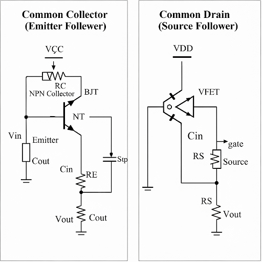
- Common Collector: In a common collector amplifier, the input is fed to the base and the output is taken from the emitter. The configuration ideally provides a voltage gain close to 1, maintaining the signal's amplitude with a high input resistance and low output resistance.
- Common Drain: Similar to the common collector, the common drain amplifier offers high input impedance and low output impedance, with the source as the output node and gate receiving the input signal.
In both cases, the key performance metrics such as gain, input/output impedances, and input capacitances are analyzed to ensure these configurations meet the necessary requirements for effective circuit design.
Youtube Videos

Audio Book
Dive deep into the subject with an immersive audiobook experience.
Introduction to Common Collector and Common Drain Amplifiers
Chapter 1 of 5
🔒 Unlock Audio Chapter
Sign up and enroll to access the full audio experience
Chapter Content
So, dear students welcome back to our NPTEL online certification course. The course title it is Analog Electronic Circuit, and now myself Pradip Mandal from E and EC Department of IIT, Kharagpur. Today’s topic of discussion is Common Collector and Common Drain Amplifiers. Based on our overall flow, let us see where we stand. We are in week-5 and we are discussing the building blocks, specifically we are going to discuss common collector amplifier and common drain amplifiers.
Detailed Explanation
This introduction sets the stage for discussing two important types of amplifiers used in analog electronic circuits: the common collector and common drain amplifiers. The speaker, Professor Pradip Mandal, emphasizes his role and the context of the course, specifying that they are in the fifth week of content, focusing on amplifier building blocks. Understanding the structure of amplifiers is crucial as it impacts their performance in circuits.
Examples & Analogies
Think of an amplifier like a water pipe system. Just as pipes can direct and manage water flow, amplifiers control and enhance electrical signals. In this course, we will explore how to build and optimize these 'pipes' for better 'water' flow in our electronic circuits.
Motivation Behind Using Common Collector and Common Drain Amplifiers
Chapter 2 of 5
🔒 Unlock Audio Chapter
Sign up and enroll to access the full audio experience
Chapter Content
We shall start with the motivation of going for this new configuration namely common collector and common drain amplifiers, and then basic operation biasing, and then analysis for specifically for voltage gain, input and output impedance of those amplifiers.
Detailed Explanation
The motivation for using common collector (BJT) and common drain (MOSFET) configurations arises from limitations experienced with previous amplification stages, such as common emitter and common source amplifiers. These limitations often include signal degradation and issues with bandwidth when connecting multiple stages of amplifiers together. By using common collector and common drain configurations, one can achieve high input impedance, low output impedance, and a voltage gain of approximately one, which prevents significant signal loss during cascading stages.
Examples & Analogies
Imagine you have multiple speakers linked together to amplify sound. If one speaker is inefficient, it can muddy the sound for all others. By using a better amplifier configuration, much like a clearer speaker setup, we ensure each part of our system works harmoniously without losing quality.
Addressing Limitations of Previous Amplifier Configurations
Chapter 3 of 5
🔒 Unlock Audio Chapter
Sign up and enroll to access the full audio experience
Chapter Content
What we have seen is that when cascading two stages by connecting the output of one CE amplifier to the input of the next CE amplifier, the input resistance and output resistance of the previous stage divide the signal. As a result, the signal arriving to the input of the second amplifier is not the same as the signal obtained in unloaded condition.
Detailed Explanation
In this chunk, the speaker describes the issues that arise when connecting multiple stages of amplifiers (common emitter amplifiers in this case). The interaction between the output resistance of the first amplifier and the input resistance of the second causes signal attenuation. Thus, the second amplifier does not receive the full signal strength that it would have in isolation, leading to degraded performance.
Examples & Analogies
This can be likened to a game of telephone. If the first person whispers a message to the next and the next person is far away or mishears it, the message can become garbled. To ensure the message remains clear, we need to strengthen the communication method, similar to how an effective amplifier configuration maintains signal integrity.
Introducing the Buffer Concept
Chapter 4 of 5
🔒 Unlock Audio Chapter
Sign up and enroll to access the full audio experience
Chapter Content
The solution is to use a buffer between these two circuits. If we have some specific buffer protecting the previous stage from the loading effects coming from the second stage, then we can say that the overall performance remains intact even if we are cascading it.
Detailed Explanation
The concept of a 'buffer' is introduced as a practical solution to the issues faced when cascading amplifiers. A buffer acts as an intermediary stage that prevents the load from affecting the previous amplifier's performance. This allows the full signal to be delivered to the next stage without degradation.
Examples & Analogies
Consider a relay race where each runner passes a baton. If the next runner is too slow or too weak, the baton might drop, slowing down the whole team. A buffer here would be like a strong athlete who ensures that the baton is passed seamlessly, maintaining the team's overall speed and performance.
Characteristics of Effective Buffer Circuits
Chapter 5 of 5
🔒 Unlock Audio Chapter
Sign up and enroll to access the full audio experience
Chapter Content
The basic requirements of this voltage amplifier are that the input resistance should be as high as possible, and the output resistance should be as small as possible. The input capacitance would also be as small as possible.
Detailed Explanation
To function effectively, buffer circuits must meet certain criteria: high input resistance to avoid signal loss, low output resistance to efficiently drive the next stage, and low input capacitance to enhance bandwidth and speed. Each of these attributes ensures that the buffer can perform its role without interfering with the signal.
Examples & Analogies
Think of a strong fan pushing air into a room. The fan's ability to draw in air (high input resistance) without letting it escape inefficiently (low output resistance) and with minimal blockage (low input capacitance) determines how well it circulates air, similar to how a good buffer enhances signal strength in electronics.
Key Concepts
-
Common Collector Amplifier: Provides high input and low output impedance.
-
Common Drain Amplifier: Functions as a buffer in MOSFET applications, offering similar impedance benefits.
-
Voltage Gain: A critical characteristic that measures signal amplification.
-
Input and Output Impedance: Vital for understanding the performance and effectiveness of amplifier stages.
Examples & Applications
In audio applications, common collector amplifiers are used to buffer signals from high impedance sources to low impedance loads.
Common drain amplifiers are crucial in RF circuits to maintain signal integrity while providing the needed voltage gain.
Memory Aids
Interactive tools to help you remember key concepts
Rhymes
If you want high input, low output too, common collector will do for you!
Stories
Imagine an audio technician helping two singers. The common collector is like the buffer who keeps the sound quality intact while allowing the voices to blend harmoniously.
Memory Tools
'HIL' - High Input, Low output, a simple way to remember the key features of these amplifiers.
Acronyms
To say it best, remember 'GAIL' - Gain Always In Line!
Flash Cards
Glossary
- Common Collector
A BJT configuration where the collector is common to both input and output, providing a high input and low output impedance.
- Common Drain
A MOSFET configuration where the drain is common, offering similar impedance characteristics as the common collector amplifier.
- Voltage Gain
The ratio of output voltage to input voltage, typically close to 1 in these configurations.
- Input Impedance
The total impedance seen by the input signal, ideally high in buffer configurations.
- Output Impedance
The impedance seen by the load connected to the output, ideally low in buffer configurations.
Reference links
Supplementary resources to enhance your learning experience.