
Motivation
Enroll to start learning
You’ve not yet enrolled in this course. Please enroll for free to listen to audio lessons, classroom podcasts and take practice test.
Interactive Audio Lesson
Listen to a student-teacher conversation explaining the topic in a relatable way.
Limitations of Common Emitter and Common Source Amplifiers
🔒 Unlock Audio Lesson
Sign up and enroll to listen to this audio lesson

Today, we'll dive into the limitations of common emitter and common source amplifiers when cascading stages. Why do you think these limitations might occur?

Maybe it's because of the way the output and input resistances interact?
Exactly! The output resistance of one stage interacts with the input resistance of the next, dividing the input signal.

So, does that mean the signal that arrives at the next stage won't be the same as input?
That's right! This situation leads to a degraded voltage gain and also affects the upper cutoff frequency.

So if we have multiple stages, the signal quality keeps decreasing?
Precisely! That’s why we need a buffer between the stages. This leads us to the next point which is the introduction of new configurations, the common collector and common drain amplifiers.
The Concept of Buffer Circuits
🔒 Unlock Audio Lesson
Sign up and enroll to listen to this audio lesson

Buffers play a crucial role in improving the cascading performance of stages. Can someone summarize what properties we want in a buffer circuit?

We want high input resistance, low output resistance, and low input capacitance.
Perfect! And along with these, what about the voltage gain?
The gain should not attenuate the signal too much, preferably close to one.
Exactly! Now, let’s link this back to the common collector and common drain configurations that can serve as our buffers.
Common Collector Configuration
🔒 Unlock Audio Lesson
Sign up and enroll to listen to this audio lesson
First, let's discuss the common collector configuration. What do you think is the primary operational feature of this amplifier?
I believe it's meant to provide a high input resistance while maintaining a low output resistance.
Exactly! This configuration helps in achieving minimal voltage loss and decent current gains. Why do you think that matters in circuit design?
If the output resistance is low, it should not load down the preceding stage!
Great insight! Also, remember that the voltage gain here is typically close to one, allowing effective signal amplification without significant degradation.
Common Drain Configuration
🔒 Unlock Audio Lesson
Sign up and enroll to listen to this audio lesson
Next, we have the common drain configuration. Similar to the common collector, what do we expect from this configuration?
Similar properties! High input resistance and low output resistance.
Exactly! This is particularly useful in MOSFET circuits. How does that differ from the BJT configuration?
I guess it’s the device physics that changes the parameters but the functionality remains largely the same.
That's a good observation! In the end, both configurations work as buffers ensuring signal integrity during cascading.
Performance Metrics of Amplifiers
🔒 Unlock Audio Lesson
Sign up and enroll to listen to this audio lesson
To wrap up our session, let's summarize the key performance metrics we discussed. Can anyone list them?
High input resistance, low output resistance, minimal input capacitance, and ensuring voltage attenuation stays minimal.
Very well! These metrics guide our design choices in analog circuits. Why do you think they are crucial in practical applications?
Because ensuring quality signal transfer between stages is key to the overall amplifier performance.
Exactly! Maintaining these principles allows us to design robust circuits that function effectively in real-world applications.
Introduction & Overview
Read summaries of the section's main ideas at different levels of detail.
Quick Overview
Standard
In this section, we explore the limitations of common emitter and common source amplifiers when cascading stages, such as degraded voltage gain and upper cutoff frequency. We introduce the common collector and common drain configurations as solutions that function as buffers, maintaining high input resistance and low output resistance to optimize amplifier performance.
Detailed
Motivation for Common Collector and Common Drain Amplifiers
This section of the lecture focuses on the significant motivation for utilizing common collector (CC) and common drain (CD) amplifier configurations in analog electronic circuits.
Limitations of Previous Configurations
In the initial part, the teacher emphasizes the limitations associated with common emitter (CE) and common source (CS) amplifiers, particularly when cascaded. The key issues identified include:
- Signal Division: Connecting the output of one CE amplifier to the input of the subsequent CE amplifier leads to the output resistance and input resistance interaction, resulting in signal loss.
- Degradation of Performance: This interaction degrades the overall voltage gain of the cascaded system and limits the upper cutoff frequency due to the formation of poles caused by output resistance of the first stage and input capacitance of the second stage.
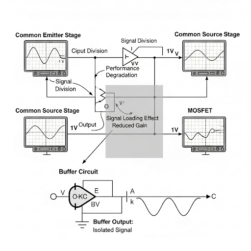
Given these constraints, the need for a buffer circuit becomes evident.
Introduction of Buffer Configurations
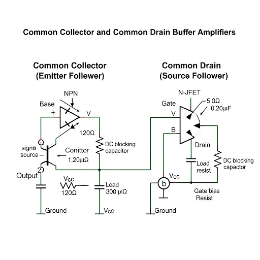
- Common Collector and Common Drain: The CC amplifier (BJT) and CD amplifier (MOSFET) configurations are proposed as buffer stages. These configurations ensure that the input resistance is kept high, output resistance low, and input capacitance minimal.
- Despite striving for voltage gain, the focus is on ensuring signal integrity rather than high gain itself.
The notions of performance metrics critical to these architectures are summarized:
1. High Input Resistance
2. Low Output Resistance
3. Minimal Input Capacitance
4. Voltage Attenuation Control
These advancements ideally lead to optimal amplifier performance when cascading stages, ensuring that the newly proposed configurations adequately serve their intended purpose.
Youtube Videos

Audio Book
Dive deep into the subject with an immersive audiobook experience.
Understanding the Limitations of Existing Amplifiers
Chapter 1 of 5
🔒 Unlock Audio Chapter
Sign up and enroll to access the full audio experience
Chapter Content
So, let us see what the basic motivation is, rather let we try to recapitulate whatever the discussion we had in the previous class. Namely, what are the limitations it was there for common emitter and common source amplifier specifically when we are cascading say two stages by connecting output of the one CE amplifier to the input of the next CE amplifier. What we have seen here, it is suppose this is the small signal equivalent circuit and then small signal equivalent circuit of the second stage, and then if you directly connect it what we have observed that the input resistance and then output resistance of the previous stage, they were dividing the signal. As a result the signal arriving to the input of the second amplifier it is not same as whatever the signal we obtained there in unloaded condition.
Detailed Explanation
In this chunk, we are recapping previous discussions about the limitations of common emitter and common source amplifiers. The issue arises when we try to connect two amplifiers, where the output of the first amplifier affects the input of the second amplifier. Specifically, the input and output resistances can create a loading effect that results in a lower signal level than expected. This loading effect (when the second amplifier draws power from the first) leads to a degradation of signal quality.
Examples & Analogies
Imagine two people trying to talk over a loud music system. If the first person speaks softly, the second person might struggle to hear them clearly. This is similar to what happens with the amplifiers; the first amplifier's output (the soft speaker) is 'loaded down' by the second amplifier, making the overall signal weaker.
Identifying the Causes of Signal Degradation
Chapter 2 of 5
🔒 Unlock Audio Chapter
Sign up and enroll to access the full audio experience
Chapter Content
And also what we have seen that the input capacitance at this the second stage, it is affecting the previous stage, namely output resistance of the previous stage and input capacitance of the second stage they were forming one pole and it was affecting the upper cutoff frequency. In fact, this is true for common source cascaded with common source amplifier also. What you have observed that the output resistance of the first stage and input resistance as well as input capacitance of the second stage they were affecting the overall performance.
Detailed Explanation
Here, we delve deeper into why the signal degradation happens. The input capacitance of the second amplifier, combined with the output resistance of the first, creates a pole that limits the frequency response of the overall system. This 'pole' is a point where the signal's strength diminishes significantly, affecting the upper cutoff frequency, which is critical for high-frequency signals in analog circuits. This implication means not only degradation in gain but also frequency response is limited.
Examples & Analogies
Think of a water pipe where the input end (of the first amplifier) has a wide opening (high output resistance), but the second pipe (input capacitance) is narrower. This bottleneck restricts the flow of water, which represents the signal's ability to carry information. If the second pipe narrows too much, the overall flow (frequency response) can drop significantly.
Proposed Solution: Using a Buffer
Chapter 3 of 5
🔒 Unlock Audio Chapter
Sign up and enroll to access the full audio experience
Chapter Content
So, what is the solution for that? It is we can use a buffer in between these two circuits and if you have some specific buffer protecting the previous stage of the first stage from the loading effect coming from the second stage, then we can say that the overall gain of the system or overall the amplifier performance it remains intact even if you are cascading it.
Detailed Explanation
To combat the signal degradation observed when cascading amplifiers, the proposed solution is to use a 'buffer' circuit. A buffer acts as an intermediary that isolates the output of the first amplifier from the input of the second. By doing so, it prevents the loading effect and maintains the overall performance of the amplifier cascade. Essentially, the buffer preserves the strength of the output signal as it drives the input of the second amplifier.
Examples & Analogies
Imagine a relay race where one runner passes a baton to another. If the first runner slows down and stumbles, the second runner won't receive the baton properly. However, if there’s a coach (the buffer) who ensures that both runners maintain their speed and separation during the handoff, the overall transfer is smoother, and both runners can perform at their best.
Requirements for Effective Buffer Operation
Chapter 4 of 5
🔒 Unlock Audio Chapter
Sign up and enroll to access the full audio experience
Chapter Content
So, what are the basic requirements of this voltage amplifier? It is that the input resistance here it will be it should be as high as possible and on the other hand input capacitance would be as small as possible. And then the output resistance of the buffer should be as small as possible. So, if we have this 3 important performance parameters are getting achieved by some circuit, then we can say that this is working as a buffer for cascading to amplifier so, whether it is CE-CE or CS-CS.
Detailed Explanation
In order for the buffer to perform effectively, several important parameters must be met: the input resistance needs to be high to ensure minimal current draw from the previous stage, the output resistance must be low to drive the next stage efficiently, and the input capacitance should be low to prevent affecting the frequency response. These three requirements are critical for the buffer to successfully isolate the stages and maintain signal integrity.
Examples & Analogies
Consider a good amplifier as a well-trained athlete who requires plenty of energy (high input resistance) without being too bulky (low output resistance and capacitance). This athlete can effectively pass his energy to the next competitor without slowing down due to baggage that would weigh him down. Meanwhile, if the buffer is properly set up, it behaves like a coach that enhances the athlete's performance by ensuring he transitions smoothly to the next stage without losing speed.
Conclusion: Transition to New Configurations
Chapter 5 of 5
🔒 Unlock Audio Chapter
Sign up and enroll to access the full audio experience
Chapter Content
So, this is the background of going for this new configuration, and let us sees how and what are the performances we are getting out of the common collector stage.
Detailed Explanation
After laying out the motivation and requirements for the new amplifier configurations, the chapter transitions to discussing the common collector and common drain configurations. These configurations are designed to meet the performance requirements that have been outlined, such as maintaining high input resistance, low output resistance, low capacitance, and minimal voltage attenuation. Essentially, they are the practical implementations to achieve optimal amplification performance.
Examples & Analogies
Imagine an upgraded sports facility where all the previous problems of noise (signal degradation), congestion (device loading), and inefficiency in transitions (performance requirements) are resolved. Each athlete (analog signal) can now perform at their peak without interference or loss, symbolizing the successful implementation of the new buffer configurations in amplifier design.
Key Concepts
-
Common Collector Amplifier: A configuration that provides amplification while preventing signal loss.
-
Common Drain Amplifier: A MOSFET configuration that acts as a buffer, maintaining signal levels.
-
Voltage Attenuation: The reduction of voltage in a cascading amplifier setup.
-
Input and Output Resistance: Critical parameters that influence the performance of amplifiers in cascading stages.
Examples & Applications
A common collector amplifier used as an interface between a low-resistance source and a high-resistance load.
Utilizing a common drain amplifier in a sensor application where minimal signal degradation is crucial.
Memory Aids
Interactive tools to help you remember key concepts
Rhymes
In cascading amplifier's way, signal's strong and won't decay; with buffers used, they play, ensuring integrity each day.
Stories
Imagine a relay race where each runner represents an amplifier stage. A strong and tall runner (the buffer) allows the next to run smoothly without losing speed.
Memory Tools
Remember the phrase 'BIR' for Buffer: B for High Input resistance, I for Low Output resistance, R for Reduced voltage attenuation.
Acronyms
Use the acronym 'HIL' to remember the desired characteristics of buffers
for High input resistance
for Ideal voltage gain close to 1
for Low output resistance.
Flash Cards
Glossary
- Common Collector Amplifier
An amplifier configuration that provides high input resistance and low output resistance, typically used as a voltage buffer.
- Common Drain Amplifier
An amplifier configuration for MOSFETs that serves a similar role to the common collector, ensuring high input resistance and low output resistance.
- Buffer
A circuit that isolates stages from one another to prevent loading effects, maintaining signal integrity.
- Voltage Gain
The ratio of output voltage to input voltage in an amplifier, ideally close to 1 for buffering applications.
- Input Resistance
The resistance seen by the input signal; higher values are preferable in amplifier design to minimize loading.
- Output Resistance
The resistance seen by the load at the output of the amplifier; lower values ensure better signal transmission.
- Cutoff Frequency
The frequency at which the output signal drops to a specific level, usually associated with the performance limits of the amplifier.
Reference links
Supplementary resources to enhance your learning experience.