
Small Signal Equivalent Circuits
Enroll to start learning
You’ve not yet enrolled in this course. Please enroll for free to listen to audio lessons, classroom podcasts and take practice test.
Interactive Audio Lesson
Listen to a student-teacher conversation explaining the topic in a relatable way.
Introduction to Small Signal Equivalent Circuits
🔒 Unlock Audio Lesson
Sign up and enroll to listen to this audio lesson

Welcome class! Today, we're diving into small signal equivalent circuits, particularly common collector and common drain amplifiers. Can anyone tell me why amplifiers are essential in electronics?

To amplify weak signals so we can use them effectively!
That's correct! Amplifiers boost weak signals. The common collector serves as a buffer, minimizing loading effects. Do you remember the key performance requirements for these buffers?

They should have high input resistance and low output resistance!
Exactly! High input resistance ensures the preceding circuit isn't loaded down. Now, what about voltage gain? How should that behave?

It should be close to 1 to avoid attenuation.
Correct! Let’s summarize the performance: We want high input resistance, low output resistance, and voltage gain near unity.
Common Collector Amplifier
🔒 Unlock Audio Lesson
Sign up and enroll to listen to this audio lesson

Now, let's focus on the common collector amplifier. Can anyone explain the basic configuration of this amplifier?

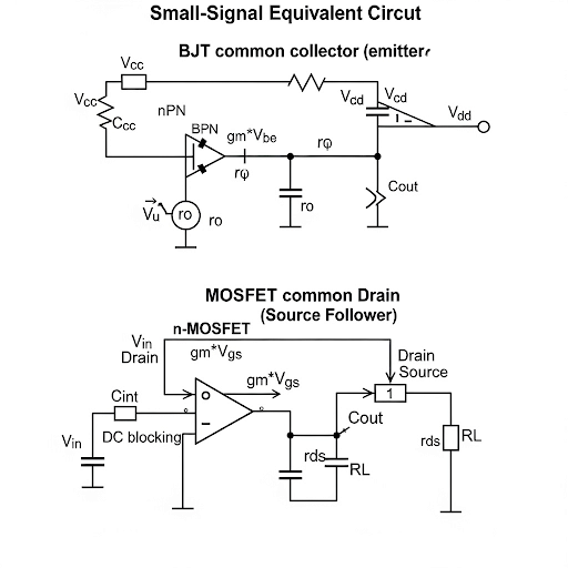
It has the emitter as the output, the base for input, and the collector typically connected to V_dd.
Great! And what happens at the emitter in terms of signal behavior?
The output signal follows the input signal closely since it acts like a voltage follower.
Exactly! This feature enables us to maintain a nearly unity voltage gain. Now, what can we say about biasing in this amplifier?
The DC biasing establishes a constant operating point, allowing the amplifier to function effectively.
Absolutely right! Biasing is crucial for operational stability.
Common Drain Amplifier
🔒 Unlock Audio Lesson
Sign up and enroll to listen to this audio lesson
Next, let’s cover the common drain amplifier. Who can describe its function?
It acts similarly to the common collector but with a MOSFET. The source is the output, and we feed the input at the gate.
Well put! And what about its input and output characteristics?
The input resistance is very high because the gate to source input impedance is nearly infinite.
That's right! And how does this amplifier behave in terms of voltage gain?
Just like the common collector, it maintains a voltage gain close to one.
Excellent! To summarize, both configurations serve as buffers ensuring minimal signal loss.
Introduction & Overview
Read summaries of the section's main ideas at different levels of detail.
Quick Overview
Standard
In this section, we explore common collector (BJT) and common drain (MOSFET) amplifiers as configurations for improving circuit performance by minimizing voltage attenuation. We examine these structures' operational principles and biasing requirements, emphasizing their high input resistance and low output resistance for effective signal amplification.
Detailed
Detailed Summary
This section dives into the fundamentals of Small Signal Equivalent Circuits, with a particular focus on common collector amplifiers for BJTs and common drain amplifiers for MOSFETs. It begins by discussing the motivation for adopting these configurations, highlighting the limitations of common emitter and common source configurations when cascading multiple stages. The text outlines how loading effects can degrade voltage gain and affect upper cutoff frequency.
The core operational principles of both configurations are delineated, showcasing their roles as buffers to isolate stages and preserve overall performance. A detailed analysis is conducted concerning voltage gain, input, and output resistances, and the impact of small-signal parameters. The section emphasizes achieving high input resistance, low output resistance, and manageable input capacitance while maintaining a voltage gain close to unity.
Through detailed circuit diagrams and calculations, the text elucidates aspects such as biasing, signal behavior at input and output, and resistive loads' effects on performance. This comprehensive discussion underlines the significance of small signal equivalent circuits in analog electronics.
Youtube Videos

Audio Book
Dive deep into the subject with an immersive audiobook experience.
Motivation for Common Collector and Common Drain Amplifiers
Chapter 1 of 4
🔒 Unlock Audio Chapter
Sign up and enroll to access the full audio experience
Chapter Content
We are looking for a buffer circuit particularly for voltage mode amplification. The important performance matrices we are looking for are: output resistance should be low, input resistance should be high, input capacitance should be as small as possible, and voltage attenuation should not be very high.
Detailed Explanation
The focus behind designing common collector and common drain amplifiers is to create a buffer circuit that maintains signal integrity when connecting two amplifier stages. In particular, we want to achieve a low output resistance, a high input resistance, and minimal input capacitance to prevent signal degradation. Additionally, we want the voltage gain around 1, meaning that the amplifier does not significantly decrease the input voltage.
Examples & Analogies
Imagine trying to fill a bucket (amplifier) with water (signal) from a hose (previous stage of amplification). If the hose (output of the first amplifier) has a small opening (high output resistance), it becomes difficult for water to flow into the bucket, resulting in a slow fill (low voltage gain). A good buffer lets water flow freely without affecting the size of the hose, ensuring efficient filling.
Basic Operation of Common Drain Configuration
Chapter 2 of 4
🔒 Unlock Audio Chapter
Sign up and enroll to access the full audio experience
Chapter Content
The common drain configuration consists of a MOSFET with the gate receiving an input signal, the source as the output terminal, and the drain generally connected to DC voltage. The output at the source follows the input signal at the gate, making the voltage gain approximately 1.
Detailed Explanation
In the common drain amplifier, the input signal is fed to the gate while the output is taken from the source. Because of the configuration, whatever signal is input to the gate, the source voltage closely matches it. This means the voltage gain of the common drain amplifier is effectively very close to 1. This operation is crucial for creating a buffer that doesn't distort the signal.
Examples & Analogies
Think about a rubber band stretched between two fingers—one finger represents the input signal (gate) and the other the output (source). No matter how you pull the rubber band (input signal), the other finger’s height (output voltage) changes in almost the same way. This characteristic ensures that the output closely follows the input, thereby functioning effectively as a signal buffer.
Voltage Gain in Common Collector and Common Drain
Chapter 3 of 4
🔒 Unlock Audio Chapter
Sign up and enroll to access the full audio experience
Chapter Content
Even with practical implementations having some conductance, the voltage gain remains approximately equal to 1. Both configurations retain the main advantage of not significantly attenuating the signal.
Detailed Explanation
Despite real-world components introducing some resistance and conductance, the overall structure allows both common collector and common drain circuits to preserve the signal strength. The goal is not to amplify the signal but rather to ensure it remains unchanged, hence the emphasis on achieving a gain close to 1.
Examples & Analogies
Think of these configurations like a professional phone call, where the call (signal) is transmitted clearly without distortion. Even if there are background noises (conductance), the person on the other side still hears you clearly, akin to how the output follows the input effectively in these amplifier configurations.
Analyzing Input and Output Resistance
Chapter 4 of 4
🔒 Unlock Audio Chapter
Sign up and enroll to access the full audio experience
Chapter Content
Using small-signal equivalent circuits helps to analyze input and output resistance in both common collector and common drain configurations. The expected behaviors are high input resistance and low output resistance.
Detailed Explanation
By applying techniques such as Kirchhoff's Current Law (KCL) to small-signal models, we can derive expressions for input and output resistances. For common collector, high input resistance is achieved due to the transistor's characteristics, while low output resistance enhances efficiency in transferring signals.
Examples & Analogies
Imagine a strong person lifting weights (input resistance) against a light weighted bar (output resistance). If the person is strong, they can handle more weights without straining, similar to how high input resistance allows better handling of incoming signals. Meanwhile, using a lighter bar lets other weights stack up easily without falling (efficient signal transfer from output).
Key Concepts
-
Common Collector: A BJT configuration offering high input resistance and low output resistance.
-
Common Drain: A MOSFET configuration providing a similar buffering function with high input impedance.
-
Biasing: Establishing the operating point of a transistor for reliable performance.
-
Voltage Gain: The ability to maintain an output level similar to the input level without significant attenuation.
-
Input/Output Resistance: Key parameters impacting signal fidelity and performance in amplifier circuits.
Examples & Applications
Common Collector Amplifier Example: Used in audio amplification to ensure the output signal from one stage can drive the input of the next without loss.
Common Drain Amplifier Example: Used in RF applications to create a buffer stage between a high-impedance source and a low-impedance load.
Memory Aids
Interactive tools to help you remember key concepts
Rhymes
In the buffer's place, we've set the pace, high input, low output, keeping signals in the race.
Stories
Imagine a busy postal worker (the amplifier) ensuring packages (signals) get delivered to the right addresses (outputs) without losing any in transit. The buffer represents a sorting facility ensuring smooth delivery.
Memory Tools
B-G-L for Buffer Gain Low: Buffer for high input resistance, Gain near unity, Low output resistance.
Acronyms
BOL
Buffer
Output Low resistance
Higher Input Resistance.
Flash Cards
Glossary
- Common Collector Amplifier
A BJT configuration where the collector is common to both input and output, providing high input resistance and low output resistance.
- Common Drain Amplifier
A MOSFET configuration where the drain is common for input and output, also known as a source follower, with high input impedance.
- Biasing
The process of setting a transistor's operating point to ensure proper function in its active region.
- Voltage Gain
The ratio of output voltage to input voltage, ideally close to 1 for buffer configurations.
- Input Resistance
The resistance seen by the input signal; high values help avoid loading down the previous stage.
- Output Resistance
The resistance seen by the load; low values are preferred for effective signal transfer.
Reference links
Supplementary resources to enhance your learning experience.