
Basic Operation and Biasing
Enroll to start learning
You’ve not yet enrolled in this course. Please enroll for free to listen to audio lessons, classroom podcasts and take practice test.
Interactive Audio Lesson
Listen to a student-teacher conversation explaining the topic in a relatable way.
Motivation for Common Collector and Drain Amplifiers
🔒 Unlock Audio Lesson
Sign up and enroll to listen to this audio lesson

Today, we're discussing the motivation behind utilizing common collector and common drain amplifiers. Can anyone tell me why these configurations might be needed instead of traditional common emitter or common source amplifiers?

I think it's because common emitter setups can face issues with signal loading when they're cascaded?
Exactly! When we cascade amplifiers, output resistance of the first stage can affect the input of the second stage, leading to signal degradation. We need a buffer. Remember this as 'High input resistance and low output resistance' — just think 'HiLo' for short term memory.

So, these configurations help maintain the signal strength?
Correct! They allow us to achieve a high input resistance, a low output resistance, and a voltage gain close to one, minimizing any attenuation.
Understanding Biasing
🔒 Unlock Audio Lesson
Sign up and enroll to listen to this audio lesson

Now let's talk about biasing in both types of amplifiers. What is the significance of proper biasing?

Isn't it to ensure the transistor operates in the active region?
That's right! Biasing keeps the transistor operational for proper amplification. For common collector stages, we stabilize the emitter voltage, which indirectly supports the base voltage adjustments.

How does that work in a common drain setup?
In a common drain, biasing ensures that the gate voltage allows the source to follow closely, making the output signal equal to the input with minimal delay. This means we can achieve signals almost at the same amplitude with a voltage gain of about 1.
Performance Analysis
🔒 Unlock Audio Lesson
Sign up and enroll to listen to this audio lesson
Next, let’s discuss how to evaluate the performance of these amplifiers. What metrics do we need to consider?
We should look at voltage gain and input/output impedance?
Exactly! The voltage gain should be high enough to amplify the signal without distortion, ideally close to 1. Also, we'd want input impedance to be high and output impedance low. Can anyone share how we could derive these values?
We can use KCL and small signal equivalent circuits to analyze the parameters.
Good thinking! This analytical approach helps clarify the performance characteristics and ensures we meet design criteria.
Practical Considerations
🔒 Unlock Audio Lesson
Sign up and enroll to listen to this audio lesson
Finally, what practical challenges might we face when implementing these configurations?
There could be issues with component tolerances affecting performance, right?
Absolutely! Variability in component values can affect the gain and biasing stability. Therefore, understanding the practical layout is essential for reliable operation.
Should we always use a buffer when cascading stages?
In most cases, yes, to avoid loading issues. Always remember the 'HiLo' principle we discussed—it's key in practical amplifier design.
Introduction & Overview
Read summaries of the section's main ideas at different levels of detail.
Quick Overview
Standard
The section explains the motivation for using common collector and common drain amplifier configurations, detailing their operation, biasing requirements, and performance parameters like voltage gain and impedance.
Detailed
Basic Operation and Biasing
In this section, we explore the fundamental principles underpinning common collector (BJT) and common drain (MOSFET) amplifier configurations. These designs arise from the need to address loading issues and signal integrity when cascading amplifiers, particularly in ensuring that input and output impedances are favorable to maintain voltage gains.
We begin by discussing the limitations faced by common emitter and common source amplifiers, particularly when connecting multiple stages. These configurations can lead to unwanted attenuation of signal strength due to the interaction between output and input resistances, which can degrade voltage gain and limit bandwidth. To solve this problem, we introduce buffer circuits, characterized by high input resistance, low output resistance, and minimal input capacitance, to facilitate smooth signal transmission between stages.
The common collector amplifier offers approximately unity voltage gain while maintaining high input and low output resistances, and similarly, the common drain amplifier achieves these goals with MOSFET technologies. Both configurations enable enhanced performance for amplified signals while minimizing issues of signal loading and frequency response degradation. The analysis proceeds to detail voltage gains, input and output impedances, and biasing in practical circuits, establishing the theoretical background critical for amplifier design.
Youtube Videos

Audio Book
Dive deep into the subject with an immersive audiobook experience.
Introduction to Common Collector and Common Drain Amplifiers
Chapter 1 of 5
🔒 Unlock Audio Chapter
Sign up and enroll to access the full audio experience
Chapter Content
So, the concepts we are going to cover in today’s discussion it is the following. We shall start with the motivation of going for this new configuration namely common collector and common drain amplifiers, and then basic operation biasing, and then analysis for specifically for voltage gain, input and output impedance of those amplifiers and then input capacitances.
Detailed Explanation
In this chunk, we will explore the fundamental concepts of common collector and common drain amplifiers. These are configurations used in electronics to improve signal amplification while reducing the adverse effects encountered in common configurations like common emitter and common source amplifiers. We'll discuss the motivation behind using these configurations, focusing on their basic operations, biasing methods, and how they affect voltage gain, input/output impedance, and input capacitance.
Examples & Analogies
Think of a common collector amplifier like a relay. When a small signal (like pressing a button) is put in, it allows a larger signal (like turning on a light) to happen without influencing each other much. This ensures that the light turns on exactly as you expect when you press the button.
Limitations of Common Emitter and Common Source Amplifiers
Chapter 2 of 5
🔒 Unlock Audio Chapter
Sign up and enroll to access the full audio experience
Chapter Content
What we have seen here, it is suppose this is the small signal equivalent circuit and then small signal equivalent circuit of the second stage, and then if you directly connect it what we have observed that the input resistance and then output resistance of the previous stage, they were dividing the signal...
Detailed Explanation
In this chunk, we learn about limitations encountered in common emitter and common source amplifiers when cascaded. When two stages of these amplifiers are connected, their input and output resistances can divide the input signal, causing signal degradation. Additionally, the interaction between the capacitance and resistances of connected stages can form a pole affecting the amplifier's upper cutoff frequency, limiting its performance.
Examples & Analogies
Imagine two pipes connected end to end. If the first pipe has a tiny opening and water flows into it, much of the flow may be blocked as it tries to push through the second pipe, which might also have a narrow opening. The water doesn't flow smoothly, illustrating how signal degradation can happen in electronic circuits.
The Concept of Buffers
Chapter 3 of 5
🔒 Unlock Audio Chapter
Sign up and enroll to access the full audio experience
Chapter Content
So, what is the solution for that? It is we can use a buffer in between these two circuits and if you have some specific buffer protecting the previous stage of the first stage from the loading effect coming from the second stage...
Detailed Explanation
To solve the signal degradation problem, introducing a buffer between amplifier stages can help. A buffer is designed to prevent loading effects—where the output resistance of one component affects the input resistance of another, effectively isolating the stages so they can perform optimally. The buffer should have high input resistance, low output resistance, and a manageable input capacitance, allowing it to maintain signal integrity.
Examples & Analogies
Consider a traffic system where introducing a roundabout (the buffer) helps manage the flow between two busy roads (two amplifier stages). It allows cars (signals) to enter and exit without getting stuck in each other's paths, facilitating smoother traffic flow.
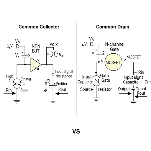
Common Collector Configuration
Chapter 4 of 5
🔒 Unlock Audio Chapter
Sign up and enroll to access the full audio experience
Chapter Content
So, let me start with the common drain first say. So, here we do have the basic common drain configuration are listed here...
Detailed Explanation
This chunk introduces the common collector configuration, detailing its operation and biasing. In this configuration, the input signal is applied to the base of a BJT, while the output is taken from the emitter. The configuration is characterized by a high input resistance and low output resistance, making it effective for voltage buffering and amplifying with minimal gain loss.
Examples & Analogies
Think of the common collector like a very efficient speaker. When a weak sound signal (like a voice) is fed into the speaker, it reproduces the sound loud enough so that it can be heard across a large hall without altering the original message. This is comparable to how a common collector amplifier works to preserve signal integrity while amplifying it.
Practical Biasing in Common Collector Configuration
Chapter 5 of 5
🔒 Unlock Audio Chapter
Sign up and enroll to access the full audio experience
Chapter Content
Note that if you observe carefully at the gate the current flow current flow of this transistor it hardly depends on the gate DC voltage...
Detailed Explanation
In this section, we emphasize the practical biasing methods used in the common collector configuration. It focuses on the gate voltage dependence, where the current may not rely heavily on the exact DC voltage applied. It discusses how slight variations in the DC voltage do not significantly impact the overall operation, allowing for flexibility in design.
Examples & Analogies
Imagine a car where the acceleration depends less on the exact pressure you apply to the gas pedal (the gate voltage) and more on the car's engine setup. As long as the engine is tuned correctly (like having a good biasing setup), the car will drive smoothly despite minor differences in pedal pressure.
Key Concepts
-
Common Collector: High input impedance and low output impedance with voltage gain close to 1.
-
Common Drain: MOSFET version of common collector with similar properties to buffer signals.
-
Biasing: Essential for ensuring proper functionality of amplifiers.
-
Loading Effects: Diminished performance due to impedance matching issues in cascaded setups.
Examples & Applications
A common collector amplifier connected as a buffer between a signal processing stage and a power amplifier stage to prevent loading.
In a common drain amplifier, the gate can be connected directly to the output of the previous stage, allowing both stages to work efficiently without interfering with each other's performance.
Memory Aids
Interactive tools to help you remember key concepts
Rhymes
In a circuit, keep it fit, common collectors do not quit, high input, low output, unity gain, that’s the key bit.
Stories
Imagine a friendly buffer, like a traffic cop, guiding signals smoothly without letting them crash into each other. That’s our common collector!
Memory Tools
Remember the 'HiLo': High input, Low output for the amplifier buffer.
Acronyms
B.O.A (Biasing, Output low, Amplification) helps you remember the key roles of amplifier design.
Flash Cards
Glossary
- Common Collector Amplifier
A transistor amplifier configuration offering high input impedance and low output impedance, primarily functioning as a buffer.
- Common Drain Amplifier
A MOSFET amplifier configuration that serves a similar purpose to the common collector, acting as a voltage buffer with low output impedance.
- Biasing
The method of applying DC voltage to the circuit to ensure that the transistor operates in the proper region.
- Loading Effect
The effect that occurs when the output impedance of one stage affects the input of the following stage, causing signal degradation.
- Voltage Gain
The ratio of output voltage to input voltage, indicating how effectively an amplifier boosts a signal.
Reference links
Supplementary resources to enhance your learning experience.