
Common Design for Testability (DFT) Techniques
Enroll to start learning
You’ve not yet enrolled in this course. Please enroll for free to listen to audio lessons, classroom podcasts and take practice test.
Interactive Audio Lesson
Listen to a student-teacher conversation explaining the topic in a relatable way.
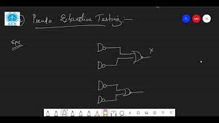
Scan-Based Testing
🔒 Unlock Audio Lesson
Sign up and enroll to listen to this audio lesson

Let's start with Scan-Based Testing. This technique involves embedding scan chains in a circuit design. Can anyone tell me what scan chains are?

I think they are links of flip-flops that allow us to shift internal signals in and out, right?
Exactly! This allows easier control and observation of internal circuitry during testing. Now, why is entering scan mode essential?

Is it because it replaces the functional data path with the scan chain?
Correct! This simplification helps detect various types of faults easily. What do you think some advantages of this method might include?

I remember that it has high fault coverage and simplifies access to internal signals.
Great! However, it also adds complexity and power consumption. Let's summarize: Scan-Based Testing unlocks complexity but comes with its challenges.
Built-In Self-Test (BIST)
🔒 Unlock Audio Lesson
Sign up and enroll to listen to this audio lesson

Now, let’s move to Built-In Self-Test or BIST. What does BIST enable in an electronic system?

It allows the system to test itself using internal diagnostics.
That’s right! This is particularly useful when external testing isn't feasible. What components are essential for BIST to function?
I think it includes a Test Pattern Generator and Response Compaction.
Exactly! This helps generate and compact results for efficient testing. How about the benefits of BIST?
It reduces the need for manual testing and can operate autonomously.
Correct, though we must note the area overhead it introduces. In summary, BIST enhances test effectiveness despite some physical drawbacks.
Boundary Scan (IEEE 1149.1, JTAG)
🔒 Unlock Audio Lesson
Sign up and enroll to listen to this audio lesson
Finally, let’s discuss Boundary Scan, defined by the IEEE 1149.1 standard. What makes this technique unique?
It allows testing of circuit interconnections without physical probing.
Correct! It uses Test Access Ports to control and observe data at boundary pins. Why might this be beneficial?
It simplifies testing for densely packed circuits.
Exactly! But remember, it only tests interconnections, not internal logic. To recap: Boundary Scan reduces testing complexity but is limited in scope.
Introduction & Overview
Read summaries of the section's main ideas at different levels of detail.
Quick Overview
Standard
DFT techniques such as Scan-Based Testing, Built-In Self-Test (BIST), and Boundary Scan are discussed, including their functionality, advantages, and challenges in ensuring electronic systems are testable and reliable.
Detailed
The section elaborates on multiple Design for Testability (DFT) techniques that help engineers incorporate testability into electronic system designs. Three key methodologies are explored: Scan-Based Testing which utilizes scan chains to access internal states during testing; Built-In Self-Test (BIST) allowing systems to diagnose themselves using internal routines; and Boundary Scan, standardized by IEEE 1149.1, enabling testing of circuit interconnects without physical access. Each strategy's advantages and challenges are examined, providing insights into how DFT enhances product reliability and reduces testing complexity.
Youtube Videos
![Design for Testability in VLSI [DFT]](https://img.youtube.com/vi/j113uLGPbUg/mqdefault.jpg)
Audio Book
Dive deep into the subject with an immersive audiobook experience.
Overview of DFT Techniques
Chapter 1 of 4
🔒 Unlock Audio Chapter
Sign up and enroll to access the full audio experience
Chapter Content
DFT incorporates several methodologies that help ensure systems can be easily tested for defects, ensuring performance and quality. Below are some of the key strategies commonly used:
Detailed Explanation
Design for Testability (DFT) refers to a set of techniques designed to improve the testability of electronic systems. DFT methodologies are integral in ensuring that systems can be examined for defects effectively, leading to better overall performance and higher quality products. The subsequent sections will discuss specific DFT techniques, each with their advantages and challenges.
Examples & Analogies
Think of DFT as a comprehensive safety inspection for a car before it's sold. Just like how technicians check every part of the car to ensure quality and safety for future drivers, DFT techniques check electronic systems to ensure they work correctly and can be tested easily.
Scan-Based Testing
Chapter 2 of 4
🔒 Unlock Audio Chapter
Sign up and enroll to access the full audio experience
Chapter Content
Scan-based testing is one of the most widely used DFT techniques. It involves embedding scan chains (sequential logic elements like flip-flops) into a circuit design, allowing access to the internal states of the system during testing.
● Scan Chains: Flip-flops in the design are linked in a series (chain), and through these chains, internal signals can be shifted in and out, allowing for easier control and observation during testing. This process enables the testing of complex sequential circuits that would otherwise be difficult to access.
● Scan Mode: The system enters scan mode during testing, replacing the functional data path with the scan chain to shift test vectors in and out of the circuit. This makes it possible to test internal logic without accessing the internal nodes physically.
● Advantages:
○ High fault coverage.
○ Simplified access to internal signals.
○ Enables detection of stuck-at faults, transition faults, and other common logic defects.
● Challenges:
○ Additional hardware overhead (scan flip-flops and multiplexers).
○ Power consumption due to the test activity.
○ Increased circuit complexity.
Detailed Explanation
Scan-based testing works by incorporating scan chains into the design of a circuit. These chains are series of flip-flops that can shift data in and out, enabling engineers to test the internal states of a circuit without physically accessing those areas. When testing, the system switches to scan mode—meaning the regular data flows are replaced by this testing mechanism. This allows for comprehensive testing, including identifying common defects like 'stuck-at faults,' where signals fail to change when they should. The method offers high fault coverage but comes with some downsides, such as requiring more hardware and potentially increasing power consumption.
Examples & Analogies
Imagine scan-based testing like making a detailed inspection of a large building using special mirrors. Instead of opening every door to check a room, inspectors can place mirrors strategically throughout the building to see what's inside without direct access, saving time and effort. However, placing those mirrors requires additional setup and might be complex.
Built-In Self-Test (BIST)
Chapter 3 of 4
🔒 Unlock Audio Chapter
Sign up and enroll to access the full audio experience
Chapter Content
Built-In Self-Test (BIST) is another key DFT strategy where test patterns and diagnostic routines are embedded within the system to enable it to test itself. This is particularly useful in situations where external test equipment is unavailable or impractical, such as in embedded systems or remote environments.
● Self-Diagnostic Capabilities: BIST allows a system to run diagnostic tests on itself, generating test patterns internally and then evaluating the results. For example, logic BIST is used to test combinational and sequential logic, and memory BIST is used to test memory units.
● Components of BIST:
○ Test Pattern Generator: Generates random or pseudo-random test patterns that simulate possible fault conditions.
○ Response Compaction: The results of the test are compressed into a signature, a compact representation of the expected behavior, which can be checked for correctness.
○ Error Detection and Reporting: Once the system tests itself, it can report any faults or deviations from the expected results.
● Advantages:
○ Enables autonomous testing without external equipment.
○ Reduces the need for manual testing or additional test hardware.
○ Useful in mission-critical applications like aerospace, automotive, and medical devices.
● Challenges:
○ Increased area overhead for additional test circuitry.
○ May not provide complete fault coverage for more complex circuits.
○ Power consumption and performance impact due to BIST logic.
Detailed Explanation
BIST is a self-testing technique, incorporating diagnostic tests and routines within the system itself, allowing it to independently check its performance. This is particularly beneficial in scenarios where it's challenging to use external testing devices, like in embedded or remote systems. BIST systems include components like a Test Pattern Generator, which creates test scenarios internally, and mechanisms for compacting and evaluating the response to identify issues. While BIST streamlines testing and reduces the dependency on manual labor, it can introduce additional area requirements for the circuitry and may also consume more power.
Examples & Analogies
Think of BIST as a self-checking alarm system in a house. Just as the system can alert homeowners about issues without requiring an outside technician to inspect it, BIST allows electronic devices to identify faults on their own. However, just like a home alarm system might miss certain issues if improperly configured, BIST may not detect every problem, especially in more complex designs.
Boundary Scan (IEEE 1149.1, JTAG)
Chapter 4 of 4
🔒 Unlock Audio Chapter
Sign up and enroll to access the full audio experience
Chapter Content
Boundary Scan is an industry-standard technique for testing the interconnections between chips and components on a printed circuit board (PCB) without requiring physical access to the connections. Defined by the IEEE 1149.1 standard (also known as JTAG), boundary scan allows for testing of the boundary pins of integrated circuits (ICs).
● Test Access Ports (TAP): Boundary scan involves connecting a TAP to the circuit, which enables the external test equipment to control and observe the data at the boundary pins of the ICs. This provides access to the internal interconnects between chips, which can be difficult to probe manually.
● Boundary Scan Cells: ICs are designed with boundary scan cells at their boundary pins. These cells allow for testing the connections between ICs without needing direct access to each pin.
● Advantages:
○ Simplifies the testing of interconnects in densely packed PCBs.
○ Eliminates the need for expensive probing equipment.
○ Standardized approach that can be used across various designs and manufacturers.
● Challenges:
○ Does not test internal logic of the circuit, just the interconnections.
○ Limited to digital circuits; does not directly apply to analog components.
Detailed Explanation
Boundary Scan is a standardized testing approach that allows engineers to test the connections of integrated circuits on a PCB without the need to physically access each connection. This method involves a Test Access Port (TAP) that connects to the circuit, aiding in controlling and observing data at the boundary pins of ICs. Boundary scan cells are designed into the ICs to facilitate testing without needing direct access to every pin. While it simplifies testing for complex boards, it primarily focuses on interconnects and does not evaluate the internal logic of circuits.
Examples & Analogies
Think of boundary scan like a monitoring system for a crowded amusement park. Instead of inspecting each ride directly (which can be difficult during busy hours), the park management uses surveillance cameras at key points to monitor the safety and connections between rides. This allows them to quickly identify and resolve any issues without having to access each ride directly. However, just as cameras can't monitor what happens inside each ride, boundary scan can only assess the connections, not the internal workings of the circuits.
Key Concepts
-
Scan-Based Testing: Uses scan chains for internal state access.
-
Built-In Self-Test (BIST): Autonomously tests systems using in-built routines.
-
Boundary Scan: Standardized method for PCB interconnect testing.
Examples & Applications
An example of Scan-Based Testing can be seen in digital circuit designs that utilize sequential logic elements to verify states.
BIST is often used in automotive or aerospace applications where in-field testing is necessary.
Memory Aids
Interactive tools to help you remember key concepts
Rhymes
To test circuits with flair, scan chains make it fair, BIST does its deed, self-tests are all we need!
Stories
Imagine an engineer named Sam who embedded testing features right in the chips he designed. This allowed his devices to check themselves without any external equipment needed and made him the go-to guy for reliable tech solutions.
Memory Tools
Remember SBB for testing: S stands for Scan-Based Testing, B for Built-In Self-Test, and B for Boundary Scan.
Acronyms
Think of DFT as 'Design For Testing' to recall its purpose.
Flash Cards
Glossary
- Design for Testability (DFT)
Techniques integrated into the design process to ensure systems are easily testable.
- ScanBased Testing
A method using scan chains to access the internal states of a circuit for testing.
- BuiltIn SelfTest (BIST)
A method where systems can self-diagnose using embedded test patterns and routines.
- Boundary Scan
Testing technique allowing examination of connection points without direct access, specified by IEEE 1149.1.
Reference links
Supplementary resources to enhance your learning experience.