
Design for Testability Strategies
Enroll to start learning
You’ve not yet enrolled in this course. Please enroll for free to listen to audio lessons, classroom podcasts and take practice test.
Interactive Audio Lesson
Listen to a student-teacher conversation explaining the topic in a relatable way.
Introduction to Design for Testability (DFT)
🔒 Unlock Audio Lesson
Sign up and enroll to listen to this audio lesson

Welcome everyone! Today, we’ll explore Design for Testability, or DFT. Can anyone tell me why DFT is crucial in designing electronic systems?

Is it because it helps make testing easier?
Absolutely! By integrating testing features into the design process itself, we simplify the verification and debugging phases, improving product quality. Let's remember that 'Design for Testability' or DFT makes testing easier—think of it as a 'Testable Design'!

What happens if we don’t consider testability during design?
Great question! Not embedding testability can lead to complex systems that are hard to debug and verify, increasing time-to-market and costs. Let's remember: 'No testing features mean more headaches later!'

Got it! So, DFT is about planning for problems before they happen.
Exactly! To summarize, thinking about DFT means designing smarter, reducing time and cost in the long run.
Scan-Based Testing
🔒 Unlock Audio Lesson
Sign up and enroll to listen to this audio lesson

Now we will dive into Scan-Based Testing. Can someone explain what scan chains are?

I think they’re series of flip-flops that help in testing internal states of a circuit.
Spot on! Scan chains allow us to shift internal signals in and out during testing. This offers high fault coverage. Does anyone remember what some challenges of using scan chains might be?
Additional hardware costs and increased complexity.
Exactly! And power consumption is a concern too. So remember: 'Scan chains = Access, but also Overheads!'
And what faults can we detect with scan-based testing?
Great question! It allows for detection of stuck-at faults and transition faults. Always keep those terms in mind, they come in handy!
Built-In Self-Test (BIST)
🔒 Unlock Audio Lesson
Sign up and enroll to listen to this audio lesson
Next, let’s talk about another critical strategy: Built-In Self-Test or BIST. What does BIST do?
Isn’t it about the system testing itself?
Correct! BIST empowers the system to generate test patterns and check results autonomously. What is one of the significant advantages of this?
It reduces the need for external testing equipment.
Well done! This feature is vital for embedded systems. However, does anyone recall the challenges associated with it?
Increased area overhead for the additional circuitry?
Right again! Keep in mind: 'BIST = Autonomy, but with Area Cost!' Let’s summarize: BIST is about making systems self-sufficient in testing.
Boundary Scan
🔒 Unlock Audio Lesson
Sign up and enroll to listen to this audio lesson
Now, how about we explore Boundary Scan? What is it designed for?
It’s for testing interconnections between chips on a PCB without needing physical access.
Exactly! It uses the IEEE 1149.1 standard, allowing access to chip boundary pins for testing. What advantage does this offer?
It simplifies the testing process of densely packed PCBs.
Correct again! However, what’s a limitation of Boundary Scan?
It only tests the interconnections and not the internal logic.
Exactly! Always remember: 'Boundary Scan = Access to Pins, but not Internal Logic!' Let’s summarize: useful for interconnect testing, but not a complete solution.
Introduction & Overview
Read summaries of the section's main ideas at different levels of detail.
Quick Overview
Standard
Design for Testability (DFT) incorporates various methodologies to simplify the testing of electronic systems, particularly as they become more complex. The section discusses techniques such as Scan-Based Testing, Built-In Self-Test (BIST), and Boundary Scan, along with the advantages and challenges of each, to optimize testing efficiency and improve product reliability.
Detailed
Design for Testability (DFT) Strategies
DFT is an essential practice integrated into modern electronic system design, focusing on embedding testability features during the design phase. This ensures efficient verification and debugging, thus enhancing product quality, reducing time-to-market, and lowering costs.
8.1 Introduction to DFT Strategies
DFT is vital as electronic circuits grow in complexity. Effective DFT strategies help ensure high-quality and reliable products by anticipating testing requirements in the design process.
8.2 Common DFT Techniques
8.2.1 Scan-Based Testing
Scan-based testing allows access to internal states of a circuit via scan chains, facilitating fault detection with advantages such as high fault coverage while facing challenges like power consumption.
8.2.2 Built-In Self-Test (BIST)
BIST provides self-diagnostic capabilities, where systems test themselves using internally generated patterns, useful in scenarios where external testing is impractical. Its challenges involve area overhead and potential incomplete fault coverage.
8.2.3 Boundary Scan (IEEE 1149.1, JTAG)
Boundary Scan allows testing of interconnections without physical access to the pins, simplifying PCB testing but only covers interconnections, not internal logic.
8.3 Additional DFT Strategies
8.3.1 Test Pattern Generation (TPG) and ATPG
Automated tools for generating test patterns enhance fault detection during testing, with challenges related to computational expense for large designs.
8.3.2 Design for Manufacturability (DFM) and Design for Reliability (DFR)
These strategies focus on creating designs that are easier to manufacture and more reliable, minimizing defects and extending product longevity.
8.4 Optimizing DFT Strategies for Efficient Testing
8.4.1 Test Compression
Test compression techniques help reduce the data volume needed for testing, mitigating time and cost issues, essential for large systems.
8.4.2 Testable Design Architecture
Designing with testability in mind enhances testing efficiency through modular structures and improved observability.
8.5 Conclusion
Overall, implementing DFT strategies is critical for ensuring that electronic systems are efficiently tested, enhancing their reliability and performance while facing the challenges of complexity and overhead.
Youtube Videos
![Design for Testability in VLSI [DFT]](https://img.youtube.com/vi/j113uLGPbUg/mqdefault.jpg)

Audio Book
Dive deep into the subject with an immersive audiobook experience.
Introduction to Design for Testability (DFT) Strategies
Chapter 1 of 7
🔒 Unlock Audio Chapter
Sign up and enroll to access the full audio experience
Chapter Content
Design for Testability (DFT) is a crucial practice in modern electronic system design that integrates testability features into the design process itself. By considering testing requirements during the design phase, DFT strategies help simplify the process of verifying and debugging a system, ensuring higher product quality, reduced time-to-market, and lower testing costs. As electronic circuits, particularly system-on-chip (SoC) and integrated circuits (ICs), become increasingly complex, efficient testability strategies are essential to meet the rising demand for high-quality, reliable products.
Detailed Explanation
Design for Testability (DFT) strategies encompass methods that integrate testing features into electronic designs during the initial design phase. This proactive approach leads to simpler verification and debugging processes, enhancing product quality and reducing time and costs associated with testing. As electronic systems grow in complexity, like integrated circuits and system-on-chip designs, the need for efficient DFT strategies escalates to satisfy market demands for high reliability and quality.
Examples & Analogies
Think of DFT like building a house with planned access points for maintenance. Just as having accessible utility areas makes it easier to service your home, incorporating test features in electronic designs makes it easier to identify and fix issues before they become major problems.
Key Strategies in Design for Testability
Chapter 2 of 7
🔒 Unlock Audio Chapter
Sign up and enroll to access the full audio experience
Chapter Content
This chapter explores the various Design for Testability (DFT) strategies that engineers use to enhance the testability of electronic systems. We will delve into the common techniques, their benefits, and challenges, focusing on how these strategies are implemented in digital circuits, embedded systems, and larger SoC designs.
Detailed Explanation
The chapter offers a comprehensive overview of DFT strategies. It outlines several common techniques engineers utilize to improve testability, examining their benefits and challenges. These strategies are particularly relevant to digital circuits, embedded systems, and complex system-on-chip designs, which are increasingly prevalent in technology today.
Examples & Analogies
Imagine a toolkit for maintaining a car. Each tool is designed for a specific task, making it easier to fix issues. Similarly, DFT strategies are like tools for engineers, helping them tackle different challenges in electronic system testing with efficiency and precision.
Common Design for Testability (DFT) Techniques: Overview
Chapter 3 of 7
🔒 Unlock Audio Chapter
Sign up and enroll to access the full audio experience
Chapter Content
DFT incorporates several methodologies that help ensure systems can be easily tested for defects, ensuring performance and quality. Below are some of the key strategies commonly used:
Detailed Explanation
DFT includes a variety of methodologies aimed at facilitating easier testing of electronic systems. These methodologies enable the identification of defects, ultimately leading to improved performance and quality of the end product. Engaging with these strategies helps create robust electronic systems that meet quality standards.
Examples & Analogies
Think about going to a doctor for a check-up. They use different methods to determine your health, such as blood tests, blood pressure checks, and imaging. These techniques help identify health issues early on. Similarly, DFT techniques help engineers assess the functionality of electronic components, uncovering potential problems before they cause failures.
Scan-Based Testing
Chapter 4 of 7
🔒 Unlock Audio Chapter
Sign up and enroll to access the full audio experience
Chapter Content
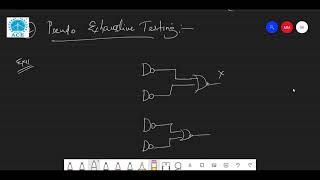
Scan-based testing is one of the most widely used DFT techniques. It involves embedding scan chains (sequential logic elements like flip-flops) into a circuit design, allowing access to the internal states of the system during testing.
● Scan Chains: Flip-flops in the design are linked in a series (chain), and through these chains, internal signals can be shifted in and out, allowing for easier control and observation during testing. This process enables the testing of complex sequential circuits that would otherwise be difficult to access.
● Scan Mode: The system enters scan mode during testing, replacing the functional data path with the scan chain to shift test vectors in and out of the circuit. This makes it possible to test internal logic without accessing the internal nodes physically.
● Advantages:
○ High fault coverage.
○ Simplified access to internal signals.
○ Enables detection of stuck-at faults, transition faults, and other common logic defects.
● Challenges:
○ Additional hardware overhead (scan flip-flops and multiplexers).
○ Power consumption due to the test activity.
○ Increased circuit complexity.
Detailed Explanation
Scan-based testing provides a structured approach to accessing internal states of a circuit by embedding scan chains made of flip-flops. These chains facilitate the entry of test signals and make it easier to observe how the circuit behaves during tests. The process allows engineers to thoroughly test complex circuits without physically accessing each part. While it offers high fault detection rates and simplifies testing, engineers must consider additional hardware needs and potential increases in complexity and power use.
Examples & Analogies
Imagine a system of pipes in a building that need to be checked for leaks. Instead of cutting open walls to inspect each pipe, you install a network of clear tubes (scan chains) that allow you to see directly into the system. You can run water through the tubes and spot leaks easily without major renovations. Similarly, scan-based testing enables engineers to observe circuit behavior efficiently.
Built-In Self-Test (BIST)
Chapter 5 of 7
🔒 Unlock Audio Chapter
Sign up and enroll to access the full audio experience
Chapter Content
Built-In Self-Test (BIST) is another key DFT strategy where test patterns and diagnostic routines are embedded within the system to enable it to test itself. This is particularly useful in situations where external test equipment is unavailable or impractical, such as in embedded systems or remote environments.
● Self-Diagnostic Capabilities: BIST allows a system to run diagnostic tests on itself, generating test patterns internally and then evaluating the results. For example, logic BIST is used to test combinational and sequential logic, and memory BIST is used to test memory units.
● Components of BIST:
○ Test Pattern Generator: Generates random or pseudo-random test patterns that simulate possible fault conditions.
○ Response Compaction: The results of the test are compressed into a signature, a compact representation of the expected behavior, which can be checked for correctness.
○ Error Detection and Reporting: Once the system tests itself, it can report any faults or deviations from the expected results.
● Advantages:
○ Enables autonomous testing without external equipment.
○ Reduces the need for manual testing or additional test hardware.
○ Useful in mission-critical applications like aerospace, automotive, and medical devices.
● Challenges:
○ Increased area overhead for additional test circuitry.
○ May not provide complete fault coverage for more complex circuits.
○ Power consumption and performance impact due to BIST logic.
Detailed Explanation
Built-In Self-Test (BIST) empowers a system to independently conduct tests and diagnose its performance. This method is especially beneficial in scenarios where conventional testing tools are impractical, enabling self-contained testing capabilities. BIST includes components like test pattern generators that create specific test signals, and response compaction techniques that summarize test results for quick assessment. While it promotes independence from external testing means, it introduces challenges such as extra circuitry requirements and potential coverage limitations.
Examples & Analogies
Consider a car with an onboard self-diagnostic system that alerts drivers about engine problems. Instead of taking the car to a mechanic for an assessment, the car runs its own tests and displays any issues. This self-testing capability mirrors how BIST allows systems to evaluate their condition independently, which is particularly advantageous in remote or critical applications.
Boundary Scan (IEEE 1149.1, JTAG)
Chapter 6 of 7
🔒 Unlock Audio Chapter
Sign up and enroll to access the full audio experience
Chapter Content
Boundary Scan is an industry-standard technique for testing the interconnections between chips and components on a printed circuit board (PCB) without requiring physical access to the connections. Defined by the IEEE 1149.1 standard (also known as JTAG), boundary scan allows for testing of the boundary pins of integrated circuits (ICs).
● Test Access Ports (TAP): Boundary scan involves connecting a TAP to the circuit, which enables the external test equipment to control and observe the data at the boundary pins of the ICs. This provides access to the internal interconnects between chips, which can be difficult to probe manually.
● Boundary Scan Cells: ICs are designed with boundary scan cells at their boundary pins. These cells allow for testing the connections between ICs without needing direct access to each pin.
● Advantages:
○ Simplifies the testing of interconnects in densely packed PCBs.
○ Eliminates the need for expensive probing equipment.
○ Standardized approach that can be used across various designs and manufacturers.
● Challenges:
○ Does not test internal logic of the circuit, just the interconnections.
○ Limited to digital circuits; does not directly apply to analog components.
Detailed Explanation
Boundary scan is a technique governed by the IEEE 1149.1 standard that simplifies testing of connections between electronic components on a PCB by allowing access to the boundary pins of integrated circuits. Through Test Access Ports (TAP), engineers can send commands to check connections between components without needing to directly probe each pin, which is particularly helpful in high-density designs. While boundary scan presents significant advantages in terms of accessibility and standardization, it does not evaluate internal circuit logic as part of the testing process and is primarily pertinent to digital circuits.
Examples & Analogies
Think of boundary scan like a security camera monitoring the entrances of a building. The camera (TAP) can capture activity at the entrance points but can't show what's happening inside. Similarly, boundary scan can observe interactions between components but doesn't delve into their internal workings.
Conclusion of Design for Testability Strategies
Chapter 7 of 7
🔒 Unlock Audio Chapter
Sign up and enroll to access the full audio experience
Chapter Content
Design for Testability (DFT) is an essential approach in modern electronics, ensuring that systems are easier to test, debug, and verify. Strategies like scan-based testing, BIST, boundary scan, and test pattern generation have become standard tools in circuit design. While these techniques offer significant advantages in terms of fault detection, testing speed, and cost reduction, they come with challenges such as increased area overhead and power consumption. Optimizing DFT strategies through methods like test compression, hierarchical testing, and design for manufacturability can help mitigate these challenges while ensuring high-quality and reliable products.
Detailed Explanation
In conclusion, Design for Testability (DFT) is a critical methodology for simplifying the testing and verification processes in electronic design. Techniques such as scan-based testing, BIST, and boundary scan form a foundation of modern electronic testing, yielding benefits such as enhanced fault detection and improved efficiency. However, engineers must also navigate challenges including potential increases in size and power needs, which can be mitigated through approaches like test compression and modular testing strategies.
Examples & Analogies
Think of DFT as a well-organized toolkit for an engineer. Just as a well-stocked toolset helps to solve various issues quickly and effectively, DFT strategies equip engineers with necessary techniques to address a range of testing challenges in electronics, ensuring products are reliable and of high quality.
Key Concepts
-
Design for Testability (DFT): The integration of test features into system design for enhanced testing.
-
Scan-Based Testing: A technique involving scan chains for internal signal access.
-
Built-In Self-Test (BIST): Allows systems to perform self-diagnostics.
-
Boundary Scan: Enables testing of interconnections without direct access to the pins.
-
Test Pattern Generation (TPG): The creation of input vectors for circuit testing.
-
Automated Test Pattern Generation (ATPG): Tools used for generating efficient test patterns.
-
Design for Manufacturability (DFM): Strategies focusing on simplifying the manufacturing process.
-
Design for Reliability (DFR): Ensuring long-term reliability in designs.
-
Test Compression: Techniques to reduce the amount of test data generated.
Examples & Applications
Scan-Based Testing allows a complex circuit to be tested for internal faults without direct access, simplifying fault detection.
In BIST, an embedded test pattern generator can allow an embedded system to check its memory units without external tools.
Boundary Scan enables testing connections between tightly packed ICs on a PCB, reducing the need for manual probing.
Memory Aids
Interactive tools to help you remember key concepts
Rhymes
For testing to be neat, make design testable and sweet.
Stories
Imagine designing a secret room but planning for inspectors to check it later. That’s DFT—making it easy for testing when it’s time!
Memory Tools
Remember DFT as 'Design, Fault-test, Testability'.
Acronyms
DFT = Design for Fault Testing.
Flash Cards
Glossary
- Design for Testability (DFT)
Strategies incorporated during the design phase to simplify tests of electronic systems.
- ScanBased Testing
A DFT technique that uses scan chains to allow access to internal circuit states during testing.
- BuiltIn SelfTest (BIST)
A strategy where devices can test themselves using internal diagnostics.
- Boundary Scan
An industry-standard method for testing connections between chips without direct access.
- Test Pattern Generation (TPG)
The process of generating input vectors for testing circuits.
- Automated Test Pattern Generation (ATPG)
Automatic generation of efficient test patterns for circuit testing.
- Design for Manufacturability (DFM)
A design approach that focuses on ease of manufacturing.
- Design for Reliability (DFR)
Designing systems to improve their reliability over time.
- Test Compression
Techniques used to reduce the volume of test data needed during testing.
Reference links
Supplementary resources to enhance your learning experience.