Summary of Key Concepts
Interactive Audio Lesson
Listen to a student-teacher conversation explaining the topic in a relatable way.
FPGA Architecture Components
🔒 Unlock Audio Lesson
Sign up and enroll to listen to this audio lesson

Today, we're focusing on the architecture of FPGAs. Can anybody name some of the key components of FPGA architecture?

There's logic blocks and I/O blocks!

Correct! Logic blocks are crucial. They include Lookup Tables, flip-flops, and multiplexers. Does anyone know what Look-Up Tables do?

They implement Boolean functions by storing truth tables!

Excellent! Remember LUT for 'Lookup Truth'. Now, can anyone tell me how interconnects work?

Interconnects connect different logic blocks together.

Right! These are programmable links, allowing flexibility in design. In summary, FPGA architecture encompasses logic blocks, interconnects, I/O blocks, clock management, and embedded memory.
FPGA Design Flow
🔒 Unlock Audio Lesson
Sign up and enroll to listen to this audio lesson

Now let’s dive into the FPGA design flow. Can someone outline the main stages involved in designing an FPGA?

It starts with requirement analysis, right?

Exactly! After requirement analysis, we proceed to design entry using HDL like VHDL or Verilog. Who can explain what happens next?

Then comes synthesis where the HDL code gets converted into a gate-level netlist.

Perfect! Remember, GS for 'Gate Synthesis'. Next, we implement the design, which involves placing the blocks and routing them. Can anyone tell me what follows that step?

Simulation and verification to ensure everything is working properly.

Correct! Finally, it ends with programming the FPGA and testing. The design flow is crucial for effective FPGA deployment.
Challenges in FPGA Design
🔒 Unlock Audio Lesson
Sign up and enroll to listen to this audio lesson

We've talked about the design flow and its stages. What are some challenges designers face in FPGA development?

There's timing analysis, right?

Yes, timing analysis is critical for meeting clock frequencies. Can someone elaborate on why timing is so important?

If the timing is off, the design can fail to operate correctly or at all.

Exactly! And what about resource utilization?

We need to optimize how we use logic blocks and memory to ensure efficiency.

Well said! Always remember, optimizing involves striking a balance between performance and resource use.
Advanced Features of FPGAs
🔒 Unlock Audio Lesson
Sign up and enroll to listen to this audio lesson

Today’s FPGAs come with advanced features. Can anyone mention one of these features?

Embedded processors, like ARM cores?

Absolutely! This integration allows for complex systems combining hardware and software. What about I/O capabilities?

They offer high-speed I/O, which is great for data-intensive applications!

Exactly! Remember the acronym HSI for 'High-Speed I/O'. Any thoughts on DSP capabilities?

DSP blocks help process data quickly, making FPGAs ideal for things like video processing.

Well done! Advanced features significantly enhance FPGA performance and flexibility.
Introduction & Overview
Read summaries of the section's main ideas at different levels of detail.
Quick Overview
Standard
The summary of key concepts focuses on the architecture of FPGAs, including logic blocks, interconnects, I/O blocks, clock management, and embedded memory. It discusses the FPGA design flow phases and the implementation of digital systems using VHDL or Verilog while also addressing challenges such as timing analysis and debugging. Additionally, it covers advanced features like embedded processors and high-speed I/O capabilities.
Detailed
Summary of Key Concepts
This section provides a comprehensive overview of Field-Programmable Gate Arrays (FPGAs) and their capabilities. It highlights critical components of FPGA architecture, such as:
- Logic Blocks: Composed of LUTs, flip-flops, and multiplexers essential for performing combinational and sequential logic.
- Interconnects: Programmable routing resources that connect the logic blocks according to the design requirements.
- I/O Blocks: Facilitate communication with external systems, supporting multiple configurations.
- Clock Management: Includes PLLs and clock dividers for managing various clock domains.
- Embedded Memory: Critical for high-speed data processing requirements.
The FPGA design flow consists of several stages—specification, HDL design entry, synthesis, implementation, simulation, programming, and testing—all aimed at effectively developing and deploying digital systems.
Key challenges in FPGA designs include ensuring timing validity and optimizing resource utilization. Moreover, advanced features such as the integration of embedded processors and high-speed I/O blocks enhance the FPGA's flexibility and performance.
Youtube Videos


Audio Book
Dive deep into the subject with an immersive audiobook experience.
FPGA Architecture Components
Chapter 1 of 5
🔒 Unlock Audio Chapter
Sign up and enroll to access the full audio experience
Chapter Content
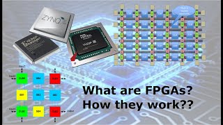
● FPGA Architecture: Includes programmable logic blocks, interconnects, I/O blocks, clock management, and embedded memory.
Detailed Explanation
This chunk summarizes the structural components that make up an FPGA. It highlights five critical elements: programmable logic blocks (the heart of the FPGA which perform computations), interconnects (which help in the routing of signals), I/O blocks (which connect the FPGA to other devices), clock management (that handles timing and synchronization), and embedded memory (local storage for data). Understanding these elements is crucial for comprehending how FPGAs operate.
Examples & Analogies
Think of the FPGA as a factory: the programmable logic blocks are the machines that perform tasks, the interconnects are the conveyor belts that move products around, I/O blocks are the doors through which raw materials come in and finished products go out, clock management is the factory manager ensuring everything runs on schedule, and the embedded memory is like a storage warehouse for materials used in manufacturing.
FPGA Design Flow
Chapter 2 of 5
🔒 Unlock Audio Chapter
Sign up and enroll to access the full audio experience
Chapter Content
● Design Flow: Includes specification, design entry (HDL), synthesis, place-and-route, simulation, programming, and testing.
Detailed Explanation
The design flow is a series of stages that a designer goes through to create an FPGA-based system. This starts with the specification stage where the desired functionality is defined. Next is the design entry, where the system is described using a hardware description language (HDL). Synthesis converts the HDL into a hardware representation. Place-and-route organizes the design onto the FPGA structure. Simulation checks functionality before implementation, followed by programming the FPGA, and finally testing to ensure everything functions correctly in hardware.
Examples & Analogies
Consider the design flow as preparing a recipe in the kitchen. You start by selecting what dish to cook (specification), gather your ingredients (design entry), follow a set of instructions to prepare the meal (synthesis), arrange everything in pots and pans (place-and-route), taste test to see if it’s good (simulation), cook it (programming), and then serve it to your guests (testing) to ensure everyone enjoys the meal.
Implementing Digital Systems
Chapter 3 of 5
🔒 Unlock Audio Chapter
Sign up and enroll to access the full audio experience
Chapter Content
● Digital Systems Implementation: Implement digital systems such as counters, state machines, and complex processors on FPGAs using VHDL or Verilog.
Detailed Explanation
This point emphasizes the capabilities of FPGAs in implementing various digital systems. Devices like counters or state machines can be programmed using languages such as VHDL or Verilog. This flexibility allows designers to create custom solutions for specific tasks or apply complex computational logic in a versatile way, making FPGAs a popular choice for many digital applications.
Examples & Analogies
Imagine a programmable robot that can perform various tasks like picking up objects, sorting them, or even cooking based on your commands. Each task can be seen as a digital system (like a counter or state machine) that the FPGA can execute, allowing the robot to adapt its functions for different jobs.
Challenges in FPGA Design
Chapter 4 of 5
🔒 Unlock Audio Chapter
Sign up and enroll to access the full audio experience
Chapter Content
● Challenges: Key challenges include timing analysis, debugging, and optimizing resource utilization.
Detailed Explanation
This chunk discusses the common hurdles faced when designing FPGA systems. Timing analysis ensures that all parts of the system operate within the correct time frames. Debugging is the process of finding and fixing errors, which can be complex in hardware. Lastly, optimizing resource utilization involves making sure the FPGA uses all its components efficiently, which can be a challenging balancing act to maintain performance without wasting resources.
Examples & Analogies
Think of these challenges like preparing for a big sports event. Timing analysis is like ensuring you train with a good schedule to be ready on time, debugging is like fixing errors in your technique before the event, and optimizing resource utilization is like making sure you eat the right foods and train enough without overdoing it so you can perform your best.
Advanced Features of Modern FPGAs
Chapter 5 of 5
🔒 Unlock Audio Chapter
Sign up and enroll to access the full audio experience
Chapter Content
● Advanced Features: Embedded processors, high-speed I/O, and DSP capabilities are key features of modern FPGAs.
Detailed Explanation
This chunk highlights the advanced functionalities that modern FPGAs offer. Embedded processors allow for more complex computations alongside programmable logic. High-speed I/O capabilities enable fast data communication with other devices. Additionally, Digital Signal Processing (DSP) features allow for efficient handling of real-time signal processing tasks, which is crucial in applications like audio and video processing.
Examples & Analogies
Think of this as upgrading a smartphone. The embedded processor is like having a powerful chip that can handle multiple apps at once. The high-speed I/O is akin to having super-fast internet connectivity, allowing for smooth downloads and streaming. Finally, the DSP capability is like having specialized software that enhances image clarity or sound quality without slowing down the device's main functions.
Key Concepts
-
FPGA Architecture: Includes components like logic blocks, interconnects, I/O blocks, and embedded memory.
-
FPGA Design Flow: The stages include requirement analysis, design entry, synthesis, implementation, simulation, and testing.
-
Challenges: Key challenges include timing analysis, debugging, and optimizing resource utilization.
-
Advanced Features: Notable advanced features include embedded processors, high-speed I/O, and DSP capabilities.
Examples & Applications
A 4-bit counter implemented on an FPGA using VHDL demonstrates how digital systems can be effectively constructed and programmed.
Utilizing high-speed I/O capabilities for a video processing application reinforces the performance advantages of modern FPGAs.
Memory Aids
Interactive tools to help you remember key concepts
Rhymes
In an FPGA, logic blocks play, interconnects keep signals at bay.
Stories
Imagine an engineer designing a spaceship using an FPGA. The logic blocks represent the engines, interconnects are the fuel lines, and the I/O blocks are the controls used outside, leading to successful launches!
Memory Tools
Remember to check your 'RDS' - Requirements, Design Entry, Simulation.
Acronyms
For components remember 'LIC' - Logic (Blocks), Interconnects, Clock (Management).
Flash Cards
Glossary
- FPGA
Field-Programmable Gate Array - A hardware device that can be configured after manufacturing.
- LUT
Lookup Table - A basic component of an FPGA that implements a Boolean function by storing truth tables.
- Design Flow
The series of stages involved in the design and implementation of a digital system on an FPGA.
- Clock Management
Techniques used in FPGAs to manage timing and synchronization across different parts of the design.
- Embedded Memory
Memory blocks included in FPGAs, essential for storing information and high-speed data processing.
- DSP
Digital Signal Processing - Specialized operations performed on signals in high-speed data applications.
Reference links
Supplementary resources to enhance your learning experience.
