
3D IC Packaging
Interactive Audio Lesson
Listen to a student-teacher conversation explaining the topic in a relatable way.
Introduction to 3D IC Packaging
🔒 Unlock Audio Lesson
Sign up and enroll to listen to this audio lesson

Good morning, class! Today, we're diving into 3D IC packaging, a technique that's revolutionizing the semiconductor industry. Can anyone tell me why space savings in packaging are vital?

Is it because electronic devices are getting smaller?
Exactly! Miniaturization is key. Now, 3D IC packaging allows us to stack multiple chips, which improves integration and performance. What do you think are some components involved in this technology?

Could it include Through-Silicon Vias?
Great point! TSVs are essential for connecting these stacked layers. They help reduce signal delay by shortening the distance between chips, which is crucial for high-speed applications.

What kind of applications use 3D IC packaging?
Excellent question! Applications include GPUs for gaming and high-performance computing. To help remember this, think of the acronym 'HIPE' for High-speed Integration in Performance Environments.

I'll remember HIPE for speed and integration!
Let's summarize—3D IC packaging enhances performance, allows for efficient use of space, and involves key components like TSVs. Next, we'll dive deeper into the benefits and explore specific examples.
The Role of Through-Silicon Vias (TSVs)
🔒 Unlock Audio Lesson
Sign up and enroll to listen to this audio lesson

Continuing our discussion, let's focus on Through-Silicon Vias. Who can describe what a TSV is?
I think it's the connection that goes through the silicon layers, right?
Exactly! TSVs connect stacked dies vertically. They are essential for allowing electrical signals to travel efficiently between layers. Why do you think this efficiency is important?
It probably makes devices faster and consumes less power?
Spot on! Now, let’s use a mnemonic to remember their benefits: 'FAST’ - Faster signals, Less Attenuation, Smaller footprint, Thermal efficiency. Can someone give an example of where TSVs are used?
Maybe in GPU designs?
Correct! GPUs leverage TSVs for performance. Remember, TSVs enhance speed and efficiency in 3D ICs, propelling advancements in many tech areas. Let's wrap up by reinforcing—TSVs are vital for high-speed, efficient 3D IC packaging.
Benefits of 3D IC Packaging
🔒 Unlock Audio Lesson
Sign up and enroll to listen to this audio lesson
Now let’s discuss the key benefits of 3D IC packaging. Can anyone share what they think these might be?
Uh, better thermal management?
Yes! That’s one major benefit. Reduced interconnect lengths lead to better thermal management. Also, 3D ICs provide higher performance by shortening signal paths. What about space savings?
Oh, right! The smaller footprint is a big deal for compact devices like smartphones.
Exactly! To remember, think of the phrase '3D Pack—Performance, Management, Space'—PMS. These benefits directly impact our modern tech. Can anyone think of a specific sector that benefits from this?
How about mobile devices?
Perfect! Mobile devices and wearables greatly benefit from 3D IC packaging. To sum up, remember the key benefits: thermal management, higher performance, and reduced footprint are pillars of this technology.
Introduction & Overview
Read summaries of the section's main ideas at different levels of detail.
Quick Overview
Standard
This section outlines the mechanics and advantages of 3D IC packaging, delving into its architecture using Through-Silicon Vias (TSVs) and exploring its benefits, including improved thermal management and integrated applications in modern technologies such as mobile devices and data centers.
Detailed
3D IC Packaging
3D IC packaging is an innovative technique that allows for the vertical stacking of multiple integrated circuits (ICs) to create a compact, three-dimensional package. This method addresses modern demands for smaller form factors without sacrificing performance. Key components, such as Through-Silicon Vias (TSVs), enable efficient electrical connections between stacked chips, enhancing signal speed and reducing power consumption.
Key Benefits
The 3D IC configuration provides several advantages:
- Thermal Management: Efficient heat dissipation becomes more feasible due to reduced interconnect lengths and improved heat transfer within the package.
- Higher Performance: Shortened paths for signal travel diminish latency, thereby increasing the overall speed of processing operations.
- Reduced Footprint: By stacking ICs, the overall size of the device can be minimized, facilitating application in space-constrained environments.
Applications
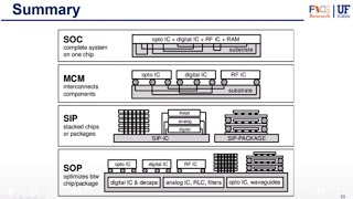
3D packaging is particularly useful in heterogeneous integration, combining different types of chips—such as processors, memory components, and sensors—into a single package suited for applications in mobile devices, high-performance computing, and Internet of Things (IoT) systems.
Youtube Videos

Audio Book
Dive deep into the subject with an immersive audiobook experience.
What is 3D IC Packaging?
Chapter 1 of 4
🔒 Unlock Audio Chapter
Sign up and enroll to access the full audio experience
Chapter Content
3D IC packaging involves stacking multiple ICs on top of each other to create a three-dimensional package. This technology allows for higher integration and smaller footprints, making it ideal for applications where space is limited.
Detailed Explanation
3D IC packaging is a modern approach to packing integrated circuits (ICs). Instead of laying them flat on a single plane, multiple ICs are stacked vertically. This stacking reduces the total area needed for the components, which is crucial in devices where space is at a premium, such as smartphones or compact electronic devices. By stacking ICs, manufacturers can also increase the overall performance due to the closer proximity of the components, which facilitates better connectivity and efficiency.
Examples & Analogies
Think of 3D IC packaging like a multi-layer cake. Instead of spreading icing on a single layer, you stack layers of cake, each with its own flavors, to create a more complex and rich dessert. Similarly, stacking ICs allows for more functionalities in a compact space.
Through-Silicon Vias (TSVs)
Chapter 2 of 4
🔒 Unlock Audio Chapter
Sign up and enroll to access the full audio experience
Chapter Content
Through-Silicon Vias (TSVs): TSVs are vertical interconnects that pass through the silicon die, allowing for electrical connections between stacked ICs. This approach reduces the distance between components, improving signal speed and reducing power consumption.
Detailed Explanation
Through-Silicon Vias (TSVs) are crucial for enabling the communication between the stacked ICs in a 3D IC packaging. They work like tiny tunnels that penetrate through the silicon layers, creating pathways for electrical connections. This dramatically decreases the distance data needs to travel between chips, which enhances the speed at which information is processed and helps conserve energy, leading to lower power usage. By improving connectivity in this way, TSVs help fulfill the high performance desired in modern electronics.
Examples & Analogies
Imagine a busy office building where departments are on different floors. If each floor (or IC) has a direct elevator (the TSV) going to every other floor, colleagues can communicate instantly without taking long stairs or walks. This efficiency mirrors the function of TSVs reducing latency and power consumption in ICs.
Benefits of 3D ICs
Chapter 3 of 4
🔒 Unlock Audio Chapter
Sign up and enroll to access the full audio experience
Chapter Content
Benefits: 3D ICs provide better thermal management, higher performance, and reduced interconnect lengths, which are critical for high-speed applications like graphics processing units (GPUs), high-performance computing (HPC), and memory devices.
Detailed Explanation
3D ICs offer multiple advantages that enhance their performance in specific applications. They improve thermal management by allowing heat to disperse more effectively due to the compact design. The shorter interconnects between components mean signals can move faster between components, which is crucial for applications that require rapid data processing, like GPUs and HPC systems. Additionally, the enhanced performance ensures that devices can handle more tasks simultaneously without faltering.
Examples & Analogies
Consider a high-performance sports car designed for speed and agility. Just like how engineers work to minimize the car's weight and improve aerodynamics for better performance, 3D ICs streamline the pathways for electrical signals, making them faster and more efficient, akin to a fast-moving car speeding on a straight road without obstacles.
Applications of 3D ICs
Chapter 4 of 4
🔒 Unlock Audio Chapter
Sign up and enroll to access the full audio experience
Chapter Content
Applications: Heterogeneous integration, where different types of chips (e.g., processors, memory, sensors) are stacked together, is a common use case. 3D ICs are used in mobile devices, data centers, IoT devices, and wearables.
Detailed Explanation
3D ICs are widely applicable in numerous modern technology sectors. The concept of heterogeneous integration allows various chip types to be stacked, enabling more complex functionalities within a single package. For example, in mobile devices, a system-on-chip (SoC) can integrate memory, processing, and sensory functions, improving performance while conserving space. Data centers, which demand high performance and processing power, benefit from 3D ICs as they require efficient data handling and storage capabilities.
Examples & Analogies
Think of a Swiss Army knife that combines multiple tools into one compact design. Just as it provides various functions without needing multiple separate tools, 3D ICs allow different chip functionalities to coexist beautifully in one package, enhancing the overall capability of devices like smartphones and smart home gadgets.
Key Concepts
-
3D IC Packaging: Stacking chips for more compact designs.
-
Through-Silicon Vias (TSVs): Key components for connecting stacked ICs.
-
Thermal Management: Ensuring efficient heat dissipation in 3D packages.
-
Interconnect Density: A measure of connectivity in packaging designs.
Examples & Applications
GPUs utilizing 3D packaging for enhanced performance in graphics processing.
Mobile devices integrating multiple functionalities through heterogeneous integration.
Memory Aids
Interactive tools to help you remember key concepts
Rhymes
3D packaging, stacked so neat, saves us space, can't be beat!
Stories
Imagine a skyscraper where every floor represents a different chip, all communicating through elevators (TSVs) that connect them together to save space and speed up transactions.
Memory Tools
Use the acronym HITE: High-speed Integration for Thermal Efficiency to remember the benefits of 3D IC packaging.
Acronyms
Remember FAST for TSV benefits
Faster
Attenuation Reduced
Smaller
Thermal efficiency.
Flash Cards
Glossary
- 3D IC Packaging
A method of stacking multiple integrated circuits in a single package to enhance performance and save space.
- ThroughSilicon Vias (TSVs)
Vertical electrical connections that pass through the silicon die, enabling connectivity between stacked ICs.
- Heterogeneous Integration
Combining different types of chips into a single package for improved functionality.
- Interconnect Density
The number of electrical connections within a defined area of a semiconductor package.
- Thermal Management
Techniques used to control the temperature of semiconductor devices to ensure reliable operation.
Reference links
Supplementary resources to enhance your learning experience.