
Introduction to Advanced Topics in IC Packaging
Interactive Audio Lesson
Listen to a student-teacher conversation explaining the topic in a relatable way.
Overview of IC Packaging Needs
🔒 Unlock Audio Lesson
Sign up and enroll to listen to this audio lesson

To start, let's talk about why IC packaging is so important. With the increasing demand for smaller and faster devices, packaging technologies must evolve. Can anyone tell me what they think 'IC packaging' means?

IC packaging is how we encase and connect integrated circuits, right?
Exactly! It's crucial for protecting the circuitry and facilitating connections. It's all about accommodating greater functionality in smaller spaces. What are some examples of devices that need this?

Phones and tablets! They are getting thinner but more powerful.
Great example! We have to consider techniques like 3D IC packaging and FOWLP to achieve that.

What do 3D IC packaging and FOWLP involve?
3D IC packaging stacks multiple chips vertically, thus reducing size and improving performance. FOWLP spreads electrical connections wider to create a thinner package. Keep these concepts in mind; they’re crucial for our next discussions!
Importance of Advanced Materials
🔒 Unlock Audio Lesson
Sign up and enroll to listen to this audio lesson

Now, let’s differentiate between traditional and advanced materials in IC packaging. Can anyone think of why materials matter in this context?

I think it has to do with heat resistance and how well they conduct electricity?
That’s correct! Advanced materials improve thermal management and signal integrity, crucial for high-performance ICs. For example, what types of substrates could be considered advanced materials?
Ceramic substrates and flexible substrates come to mind.
Exactly! Ceramic substrates offer excellent thermal properties, while flexible substrates are helpful in wearables. Can anyone summarise how this links to our packaging goals?
Better materials lead to better performance and reliability in smaller devices.
That's a perfect summary! Understanding material properties is key to advanced packaging techniques.
Overview of Advanced IC Packaging Techniques
🔒 Unlock Audio Lesson
Sign up and enroll to listen to this audio lesson
In this session, let’s dive into the specific advanced IC packaging techniques we mentioned earlier. Who remembers what 3D IC packaging involves?
It stacks chips to save space!
Exactly! Now, what about FOWLP? What does it offer over traditional packaging methods?
It's thinner and integrates connections better!
Right! Just like FOWLP, 3D packaging helps in many applications, such as GPUs and IoT devices. How do these techniques impact manufacturing?
They likely help in scaling production and may reduce costs in the long run?
Very insightful! These advanced techniques are crucial for driving costs down while enhancing device performance.
Introduction & Overview
Read summaries of the section's main ideas at different levels of detail.
Quick Overview
Standard
As demand for high-performance semiconductor devices increases, IC packaging technologies are evolving. This section discusses various advanced packaging techniques, such as 3D packaging and fan-out wafer-level packaging (FOWLP), alongside emerging materials and methodologies that enhance performance, integration, and reliability.
Detailed
Introduction to Advanced Topics in IC Packaging
As technology progresses, the semiconductor industry faces mounting demands for smaller, faster, and more energy-efficient devices, compelling advancements in Integrated Circuit (IC) packaging technologies. The evolution of IC packaging is critical to enhancing performance, ensuring reliable connections, and facilitating the miniaturization of devices.
This section addresses key advancements such as:
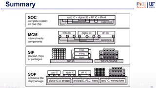
- 3D Packaging: Stackable IC designs that allow higher integration and reduced footprints, essential for compact applications.
- Fan-out Wafer-Level Packaging (FOWLP): A technique that enables smaller and thinner packages with improved electrical connections, relevant in consumer electronics.
- Advanced Materials: The use of innovative materials that enhance thermal management, signal integrity, and mechanical stability throughout various applications.
This exploration into emerging trends and methodologies sets the foundation for understanding the future direction of IC packaging in response to a rapidly evolving technology landscape.
Youtube Videos

Audio Book
Dive deep into the subject with an immersive audiobook experience.
The Need for Evolution in IC Packaging
Chapter 1 of 3
🔒 Unlock Audio Chapter
Sign up and enroll to access the full audio experience
Chapter Content
As the demand for smaller, faster, and more efficient semiconductor devices continues to grow, IC packaging technologies must evolve to meet these challenges.
Detailed Explanation
This chunk highlights the increasing demand for semiconductor devices that are not only smaller and faster but also more efficient. As technology advances, there is a constant push for these devices to fit into smaller spaces while performing at higher speeds. Therefore, the packaging techniques that house these chips need to evolve and improve continuously to meet these new demands.
Examples & Analogies
Think of it like packaging food for a picnic. If you have a bigger cooler (better IC packaging technology), you can fit more items or larger items in it. But if you have to fit everything in a smaller lunchbox (like miniaturized devices), you need to think creatively about how to arrange and package the items without compromising quality.
Goals of Advanced IC Packaging Techniques
Chapter 2 of 3
🔒 Unlock Audio Chapter
Sign up and enroll to access the full audio experience
Chapter Content
Advanced IC packaging techniques aim to address the need for higher performance, compact form factors, and reliable connections while enabling miniaturization, higher integration, and enhanced functionality in complex systems.
Detailed Explanation
This chunk explains the goals behind developing advanced IC packaging techniques. The techniques focus on achieving better performance and ensuring that the packages are small and compact. This compactness is critical for modern electronics, allowing for more integration of different functionalities within a single device, all while maintaining reliable electrical connections among components.
Examples & Analogies
Imagine a Swiss Army knife. It’s small, yet it packs various tools into one compact device. Similarly, advanced IC packaging techniques strive to integrate more functionalities into smaller sizes, enhancing the overall utility of semiconductor devices.
Overview of Emerging Trends
Chapter 3 of 3
🔒 Unlock Audio Chapter
Sign up and enroll to access the full audio experience
Chapter Content
This chapter explores emerging trends in IC packaging technologies, as well as advanced materials and techniques used to meet the evolving needs of the semiconductor industry. We will discuss 3D packaging, fan-out wafer-level packaging (FOWLP), advanced substrates, and innovative materials that are shaping the future of IC packaging.
Detailed Explanation
Here, we get an overview of what the chapter will cover. It introduces key topics like 3D packaging, fan-out wafer-level packaging, and advanced substrates, which are all innovative methods being employed in IC packaging. These trends are essential as they represent the cutting-edge solutions being implemented to fulfill the changing requirements of the semiconductor industry.
Examples & Analogies
Consider trends in smartphone design. Just like manufacturers constantly innovate with features such as foldable screens or camera advancements, the semiconductor industry is also innovating in IC packaging. This section sets the stage for similar upcoming innovations in packaging techniques, which drive efficiency and performance, akin to how smartphones continuously improve.
Key Concepts
-
Miniaturization: The trend of creating smaller devices while maintaining or improving their functionality.
-
Integration: Combining multiple functionalities into one package to enhance performance and reduce footprint.
-
Reliability: The capacity of packaging techniques to endure environmental stresses without failure.
Examples & Applications
A smartphone utilizing 3D IC packaging to host multiple functionalities, such as camera, processor, and memory in a compact form.
Fan-out wafer-level packaging used in a smartwatch to provide a thin profile while ensuring connectivity and heat management.
Memory Aids
Interactive tools to help you remember key concepts
Rhymes
To package ICs with great flair, space-saving designs are quite rare.
Stories
Imagine a tiny factory that assembles chips in layers, like a layered cake, allowing quicker passage of signals and reduced footprints.
Memory Tools
For [3D] IC packaging, remember: 'Stack high, connect fast, save space!' (SHCFSS).
Acronyms
FOWLP
'Fan Out for Wide Low Projections.'
Flash Cards
Glossary
- IC Packaging
The method of encasing and connecting integrated circuits to allow them to function within electronic devices.
- 3D IC Packaging
A technique that stacks multiple ICs vertically to create a three-dimensional package, enabling higher integration and smaller footprints.
- FanOut WaferLevel Packaging (FOWLP)
An advanced packaging technique where the IC is placed in a reconstituted wafer with connections fanned out to a larger area, allowing for a smaller and thinner package.
- Thermal Interface Materials (TIMs)
Materials used to improve thermal conductivity between ICs and heat sinks to ensure effective heat dissipation.
- Ceramic Substrates
High-performance materials used in IC packaging known for excellent thermal conductivity and high-temperature resistance.
Reference links
Supplementary resources to enhance your learning experience.