
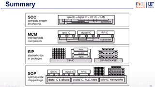
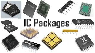
Packaging Types and Trade-offs
Interactive Audio Lesson
Listen to a student-teacher conversation explaining the topic in a relatable way.
Introduction to IC Packaging Types
🔒 Unlock Audio Lesson
Sign up and enroll to listen to this audio lesson

Today, we will discuss the importance of IC packaging types. Why do you think the packaging type is crucial in semiconductor design?

I think it affects the device's performance, right?
Exactly! The right choice impacts performance, manufacturability, and cost. There are three main types we will cover: through-hole, surface-mount, and ball grid array.

Can you remind us why different applications might need different types?
Great question! Different applications have unique requirements for mechanical strength, size, and assembly processes. Let's dive deeper.
Through-Hole Packaging
🔒 Unlock Audio Lesson
Sign up and enroll to listen to this audio lesson

Let’s talk about through-hole packaging. What are some key design features?

I believe it has long leads and is generally larger than surface-mount types.
Correct! These features lead to advantages like robustness in high-vibration environments. But remember, there's a trade-off!

What’s the trade-off here?
The larger size means less component density, leading to increased board size. Can someone give examples of where through-hole types might be used?
I think they are used in high-current applications like power supplies?
Absolutely! Excellent recall.
Surface-Mount Packaging
🔒 Unlock Audio Lesson
Sign up and enroll to listen to this audio lesson
Moving on to surface-mount technology. What do you all remember about its design features?
It has flat leads and is smaller than through-hole components!
Exactly! This allows for higher density and faster assembly. But what are some limitations?
It’s not as mechanically strong, and repairing can be a hassle!
Spot on! That’s why it’s popular in consumer electronics. Can anyone think of a specific product?
Smartphones! They need to be compact and efficient.
Well done! Compactness is indeed key.
Ball Grid Array (BGA)
🔒 Unlock Audio Lesson
Sign up and enroll to listen to this audio lesson
Lastly, let's discuss Ball Grid Array packaging. What makes it unique?
It uses solder balls instead of leads!
Correct! This design allows for smaller and denser packages. What about its advantages?
Better electrical performance due to shorter interconnects.
Exactly! But what’s a major challenge with BGA?
The hidden solder balls make repair and inspection difficult?
Right again! That's a significant trade-off for its high performance.
Trade-offs in Selecting Packaging Types
🔒 Unlock Audio Lesson
Sign up and enroll to listen to this audio lesson
To wrap up, let's discuss the trade-offs involved in selecting packaging types. Why is this balance important?
So we can match the right packaging with the project needs, like performance and cost?
Exactly! For instance, choosing between through-hole for mechanical strength or BGA for compactness requires careful consideration.
And consumer electronics would favor surface-mount for size!
Very good! Recapping these trade-offs empowers engineers to make informed packaging selections.
Introduction & Overview
Read summaries of the section's main ideas at different levels of detail.
Quick Overview
Standard
In this section, we discuss the importance of selecting the appropriate IC packaging type, detailing three common types: through-hole, surface-mount, and ball grid array. Each type is analyzed through its design features, advantages, disadvantages, and specific applications, helping engineers navigate the trade-offs involved in the selection process.
Detailed
Detailed Summary
The selection of the right integrated circuit (IC) packaging type is crucial for optimizing semiconductor device performance and manufacturability. The section dives into three main types of IC packaging:
1. Through-Hole Packaging
- Design Features: Includes long leads and a larger size, which provides mechanical strength.
- Advantages: Offers mechanical durability and ease of manual soldering, making it suitable for high-stress applications and prototyping.
- Disadvantages: Larger footprint on PCBs and slower assembly times compared to other technologies.
- Applications: Common in high-current applications, military, and aerospace electronics.
2. Surface-Mount Packaging (SMT)
- Design Features: Components are mounted on the PCB surface, yielding smaller sizes and higher component densities.
- Advantages: Facilitates automated assembly and provides a compact design for faster manufacturing.
- Disadvantages: Lacks the mechanical strength of through-hole components and is more challenging for rework.
- Applications: Predominant in consumer electronics, automotive systems, and high-performance circuits.
3. Ball Grid Array (BGA)
- Design Features: Utilizes an array of solder balls for electrical connections, allowing for a compact design.
- Advantages: Higher pin density and better thermal/electrical performance, suitable for complex ICs.
- Disadvantages: Inspection and rework are difficult due to hidden solder balls.
- Applications: Widely used in high-performance processors, mobile devices, and networking equipment.
Trade-offs
The choice among these types involves considering performance requirements, cost, and manufacturability. Understanding these trade-offs allows engineers to select the most suitable packaging for their specific applications.
Youtube Videos


Audio Book
Dive deep into the subject with an immersive audiobook experience.
Introduction to IC Packaging Types
Chapter 1 of 17
🔒 Unlock Audio Chapter
Sign up and enroll to access the full audio experience
Chapter Content
Choosing the appropriate IC packaging type is a critical decision in the design and manufacturing process of semiconductor devices. Different packaging technologies—such as through-hole, surface-mount, and ball grid array (BGA)—offer varying advantages depending on the application, performance requirements, cost constraints, and manufacturability.
In this chapter, we will explore these three popular packaging types in detail, analyzing their design features, applications, advantages, and disadvantages. We will also discuss the trade-offs that engineers must consider when selecting the right packaging type for a given project.
Detailed Explanation
The introduction highlights the importance of selecting an appropriate packaging type for integrated circuits (ICs). It acknowledges that different technologies cater to varying needs based on factors like application specifics, performance, cost, and ease of manufacturing. The chapter promises to delve into three major packaging types—through-hole, surface-mount, and BGA—and provides an overview of what to expect in terms of design features and trade-offs in selection.
Examples & Analogies
Imagine choosing a backpack for different activities. If you’re going hiking, you need a sturdy, durable backpack (similar to through-hole packaging). For daily commuting to work or school, you might pick a lightweight, compact backpack (like surface-mount packaging). And for specific tasks like a climbing trip, you’d choose a highly specialized backpack that fits particular equipment needs (akin to BGA). Each choice caters to different requirements, just like selecting IC packaging types.
Through-Hole Packaging Overview
Chapter 2 of 17
🔒 Unlock Audio Chapter
Sign up and enroll to access the full audio experience
Chapter Content
Through-hole packaging was the standard in the early days of semiconductor packaging. In this method, components have long leads that are inserted into holes drilled through the PCB and soldered on the opposite side. This type of packaging is widely used in applications requiring high mechanical strength or easy repairability.
Detailed Explanation
Through-hole packaging is one of the oldest methods used in electronics. Here, components come with long metal leads that pass through the printed circuit board (PCB) and are soldered from underneath. This style is beneficial in situations where durability is essential or where components may need to be replaced easily, as the leads are fully accessible.
Examples & Analogies
Think of through-hole packaging like fixing something with nails instead of glue. When building a furniture piece, using nails (through-hole) might make it sturdier and easier to replace or adjust if needed, whereas glue might not offer that same strength or ease of repair when it comes to stability.
Design Features of Through-Hole Packaging
Chapter 3 of 17
🔒 Unlock Audio Chapter
Sign up and enroll to access the full audio experience
Chapter Content
Design Features of Through-Hole Packaging
- Long Component Leads: Components have long metal leads that pass through the PCB and are soldered on the opposite side.
- Large Size: Through-hole components are typically larger and bulkier compared to surface-mount counterparts.
- Higher Profile: The height of the component is greater, leading to larger vertical dimensions on the PCB.
Detailed Explanation
Through-hole packaging has specific design elements that differentiate it from other types. Long leads make soldering possible from the underside and offer a stronger mechanical connection. The size of these components tends to be larger, affecting how many can fit on a PCB. Additionally, their height requires more vertical space, which can be a constraint in compact designs.
Examples & Analogies
This is akin to building with lumber versus nails. Lumber (like through-hole components) is bulkier and strong, requiring more space and clear structures, while nails take up less space and can be integrated more swiftly into smaller designs, showcasing a contrast similar to how different packaging types function in electronic designs.
Advantages of Through-Hole Packaging
Chapter 4 of 17
🔒 Unlock Audio Chapter
Sign up and enroll to access the full audio experience
Chapter Content
- Mechanical Durability: Through-hole components are more mechanically robust, making them suitable for high-vibration environments or high-stress applications.
- Ease of Manual Soldering: Through-hole packages are easier to solder manually, making them ideal for low-volume or prototyping applications.
- Repairability: Components can be more easily replaced or repaired in the event of failure, as their leads are visible.
Detailed Explanation
There are several key advantages to through-hole packaging, including their sturdy design, which makes them ideal for settings that encounter vibration or physical stress. They are also straightforward to solder by hand, which facilitates prototyping or low-volume production. Additionally, if a component fails, it can be replaced more easily due to its visible leads.
Examples & Analogies
Imagine a robust toolbox that allows ease of repair for tools needing seasonal maintenance. Through-hole packaging is like this toolbox—it lets you access and replace tools easily, ensuring you can always keep your workspace well-functioning, similarly to how through-hole components can be accessed and replaced.
Disadvantages of Through-Hole Packaging
Chapter 5 of 17
🔒 Unlock Audio Chapter
Sign up and enroll to access the full audio experience
Chapter Content
- Larger Size: Through-hole packages take up more space on the PCB, reducing the overall component density and increasing board size.
- Slower Assembly Process: The assembly process for through-hole packages is slower compared to surface-mount technology, especially in automated manufacturing.
- Higher Cost for High Volumes: Through-hole packages are generally more expensive to manufacture in high volumes due to the more complex assembly process.
Detailed Explanation
Despite its advantages, through-hole packaging has notable drawbacks. Its size means fewer components can fit on a PCB, which can hamper design efficiency. The assembly is slower than surface-mount processes, which can increase production time. Additionally, when producing large quantities, costs can be higher due to the complexities involved in assembling these components.
Examples & Analogies
If you think of moving large furniture into a tight space, it requires more time, effort, and sometimes multiple trips. Through-hole packaging is similar; while sturdy, its larger size can sometimes slow you down in tightly designed electronic boards, ensuring more time is spent on assembling each item properly.
Applications of Through-Hole Packaging
Chapter 6 of 17
🔒 Unlock Audio Chapter
Sign up and enroll to access the full audio experience
Chapter Content
- High-Current Applications: Used in power electronics where high current handling and mechanical stability are required, such as in power supplies and power transistors.
- Prototype and Low-Volume Production: Ideal for prototyping, repair, and small-run production where ease of hand-soldering and flexibility are key.
- Military and Aerospace: Often used in applications where reliability and robustness are critical, such as in aerospace or military electronics.
Detailed Explanation
Through-hole packaging finds its niche in specific applications. They are essential in high-current electronics where stability is crucial, such as in power supplies. Their ease of hand-soldering makes them favorable in prototype settings. Additionally, industries where reliability is non-negotiable, like military or aerospace, often utilize this packaging type due to its robust nature.
Examples & Analogies
Think of a family heirloom that you only use during family gatherings—just as you wouldn’t want to risk damaging it at casual events, through-hole components are used where reliability must be assured without compromise, much like keeping cherished items safe for significant occasions.
Surface-Mount Technology Overview
Chapter 7 of 17
🔒 Unlock Audio Chapter
Sign up and enroll to access the full audio experience
Chapter Content
Surface-mount technology (SMT) is the most widely used packaging technique today. In SMT, components are mounted directly onto the surface of the PCB, eliminating the need for holes. This allows for higher component density, smaller footprint, and faster automated assembly.
Detailed Explanation
SMT is the dominant approach in modern electronics. Unlike through-hole packaging where components pass through the PCB, SMT components lie flat on the surface. This difference facilitates increased component density, allowing more parts to fit in a smaller area, and enables quicker automated assembly, benefitting mass manufacturing.
Examples & Analogies
Picture a tile backsplash in a kitchen; arranging tiles directly on the wall (SMT) allows you to place more in a limited space than using more considerable, bolt-on shelves (analogous to through-hole). Just like the tiles on a wall maximize space and efficiency, SMT makes the most of surface area on PCBs.
Design Features of Surface-Mount Packaging
Chapter 8 of 17
🔒 Unlock Audio Chapter
Sign up and enroll to access the full audio experience
Chapter Content
Design Features of Surface-Mount Packaging
- Flat Leads: SMT components have flat leads or pads that are soldered directly onto the PCB.
- Smaller Size: SMT components are typically smaller than through-hole components, allowing for higher-density packing on the PCB.
- Low Profile: These components generally have a lower profile compared to through-hole components.
Detailed Explanation
Surface-mount components feature flat leads that make them easy to solder onto flat surfaces, resulting in smaller sizes compared to through-hole variants. Their low profile is particularly advantageous in compact devices, allowing designers to enhance the density of components on a PCB.
Examples & Analogies
Think of packing a suitcase for a trip. Using compression bags (like SMT), you're able to fit more clothes in a smaller space compared to organized separate compartments which use more volume (akin to through-hole). This efficiency allows you to take what you need without sacrificing space.
Advantages of Surface-Mount Packaging
Chapter 9 of 17
🔒 Unlock Audio Chapter
Sign up and enroll to access the full audio experience
Chapter Content
- Compact Size: SMT allows for high component density, which reduces the size of the PCB and allows for smaller, more compact devices.
- Automated Assembly: SMT components are ideal for automated soldering, leading to faster manufacturing, better consistency, and lower labor costs.
- Higher Performance: Shorter interconnection lengths and reduced parasitic inductance in SMT designs help improve high-speed signal transmission.
- Lower Cost in High Volumes: For high-volume production, SMT components are cost-effective due to automation and reduced material usage.
Detailed Explanation
The benefits of surface-mount technology are significant. Its compact size facilitates a higher density of components, benefiting the overall design by saving space. Automated manufacturing speeds up production, ensures uniform results, and reduces costs in the long run. Because SMT minimizes the length of connections, it also enhances signals, which is crucial for high-speed applications.
Examples & Analogies
Using mass transit instead of personal cars can save time and resources when traveling through a busy city. Similarly, SMT enables efficient production and powerful performance, ensuring that electronic devices are not only compact but also quicker than traditional methods, maximizing efficiency like public transport does during peak hours.
Disadvantages of Surface-Mount Packaging
Chapter 10 of 17
🔒 Unlock Audio Chapter
Sign up and enroll to access the full audio experience
Chapter Content
- Mechanical Strength: SMT components lack the mechanical durability of through-hole components, making them unsuitable for high-vibration or high-stress applications.
- Repair and Rework: While reflow soldering is efficient for assembly, repair and rework of SMT components are more difficult and require specialized tools such as hot air rework stations or soldering irons.
- Limited Power Handling: SMT components typically have lower power handling capabilities than through-hole components due to their smaller size and lower profile.
Detailed Explanation
There are key challenges associated with surface-mount technology. The components are generally less sturdy than through-hole types, making them vulnerable in high-vibration settings. Repairing SMT components can be tricky since it often requires specialized tools. Furthermore, due to their smaller size, they can handle less power, which might limit their use in high-demand scenarios.
Examples & Analogies
Consider a delicate piece of jewelry made from fine metal, much like SMT components. While beautiful and efficient, they need more careful handling and aren’t built for rugged use, thus giving an insight into how their design may not be optimal for high-stress environments, just as good jewelry isn’t suitable for every occasion.
Applications of Surface-Mount Packaging
Chapter 11 of 17
🔒 Unlock Audio Chapter
Sign up and enroll to access the full audio experience
Chapter Content
- Consumer Electronics: Used in nearly all consumer electronics, such as smartphones, tablets, and televisions, where compactness and high-density packing are required.
- Automotive and Industrial Electronics: Widely used in automotive systems, medical devices, and industrial controllers due to the need for efficient and reliable mass production.
- High-Performance Circuits: SMT is ideal for high-frequency, high-speed applications such as RF circuits, processors, and memory modules.
Detailed Explanation
Surface-mount packaging is incredibly popular for consumer electronics because it maximizes space, essential for compact devices. This technology also finds a home in automotive and industrial electronics where production efficiency must remain high. Furthermore, SMT is favored for high-performance applications that require quick signal transmission and lower delays.
Examples & Analogies
Using smartphones as an example shows how small improvements in design can lead to major practical benefits. The general structure of high-frequency radios in our phones, enabled by SMT, ensures that we can connect seamlessly without the bulky designs of older technologies.
Ball Grid Array (BGA) Overview
Chapter 12 of 17
🔒 Unlock Audio Chapter
Sign up and enroll to access the full audio experience
Chapter Content
Ball Grid Array (BGA) is an advanced packaging technique that uses an array of solder balls as interconnection points instead of pins or leads. BGA packages offer higher performance, better thermal management, and a more compact design compared to traditional packaging types.
Detailed Explanation
BGA is a sophisticated packaging method that utilizes a grid of solder balls to make connections between the IC and PCB. This modern technique provides better performance and thermal management while allowing for a more compact form factor compared to traditional packaging models.
Examples & Analogies
Think about a modern tablet with a sleek design; its smooth finish without protruding elements is similar to the compact nature of BGAs that use ball connections instead of traditional pins. This technology has revolutionized how we think about space and performance in tech devices.
Design Features of BGA Packaging
Chapter 13 of 17
🔒 Unlock Audio Chapter
Sign up and enroll to access the full audio experience
Chapter Content
Design Features of BGA Packaging
- Solder Balls: BGA packages have an array of solder balls at the bottom of the package, which are reflowed to connect the IC to the PCB.
- High Pin Count: BGA allows for high pin-count packages in a compact space, making it suitable for high-performance ICs.
- Low Profile: BGA components have a low profile compared to other packaging types, which allows for better integration in high-density designs.
Detailed Explanation
BGAs feature several key design characteristics, such as solder balls that enable connections between the IC and the PCB. They accommodate a high number of connections in a limited space, which is crucial for advanced ICs. The low profile of BGA components allows them to fit seamlessly into high-density design layouts.
Examples & Analogies
Think of how a multi-storey office block utilizes vertical space efficiently. Just like these buildings maximize capacity and functionality without unnecessary height that takes away from urban beauty, BGA designs offer space-efficient solutions for complex electronics.
Advantages of Ball Grid Array Packaging
Chapter 14 of 17
🔒 Unlock Audio Chapter
Sign up and enroll to access the full audio experience
Chapter Content
- Higher Pin Density: BGA allows for higher pin count and smaller packages, making it ideal for complex ICs such as processors and memory devices.
- Better Thermal Performance: The large surface area of BGA packages provides improved heat dissipation compared to traditional packages.
- Improved Electrical Performance: Shorter interconnect lengths result in lower inductance and resistance, which improves signal integrity, especially in high-speed circuits.
- Smaller Footprint: BGA packages are more compact than other types, which is crucial for devices requiring miniaturized designs.
Detailed Explanation
The advantages of BGA are clearly notable. With a high pin density, it allows manufacturers to create smaller packages, enhancing performance capabilities. Its design facilitates effective heat dissipation and superior electrical performance due to reduced interconnect lengths. This reduction in size and weight allows BGA to remain competitive in a miniaturized electronics market.
Examples & Analogies
Consider a high-end sports car with a compact design that allows for excellent speed and handling without unnecessary weight. BGAs achieve a similar effect in electronics, ensuring high performance in a small package, maximizing efficiency much like the engineering behind a performance vehicle.
Disadvantages of Ball Grid Array Packaging
Chapter 15 of 17
🔒 Unlock Audio Chapter
Sign up and enroll to access the full audio experience
Chapter Content
- Inspection and Rework: One of the main disadvantages of BGA is that the solder balls are not visible after soldering, making inspection and rework difficult. Special X-ray inspection is required.
- Complex Assembly: BGA assembly requires precise alignment during placement and soldering, which adds complexity and cost to the manufacturing process.
Detailed Explanation
While BGA offers several benefits, it also has challenges. The hidden solder balls raise difficulties in inspections and repairs, necessitating specialized equipment. Additionally, the complexity of assembly requires higher accuracy during manufacturing, which can translate to increased costs.
Examples & Analogies
Think of trying to find a needle in a haystack; once buried, the needle (representing the solder balls) is almost impossible to detect. BGA's hidden connections require careful attention during both assembly and maintenance, similar to needing a calibrated eye in order to avoid losing track of something valuable.
Applications of Ball Grid Array Packaging
Chapter 16 of 17
🔒 Unlock Audio Chapter
Sign up and enroll to access the full audio experience
Chapter Content
- High-Performance Processors: BGAs are commonly used in microprocessors, memory ICs, and GPUs, where high pin count and thermal management are essential.
- Mobile Devices and Consumer Electronics: BGAs are widely used in smartphones, tablets, and gaming consoles where small size, high performance, and efficient heat dissipation are required.
- Networking Equipment: BGAs are often found in routers, switches, and networking ICs due to their ability to handle high-speed signals and high-density connections.
Detailed Explanation
BGAs serve vital roles in high-performance applications, such as microprocessors and memory chips, where capabilities are crucial. Their compact form also fits well within mobile technology, balancing function with size. Additionally, network hardware often relies on BGAs due to their ability to manage high signal speeds, marking a clear impact across various industry domains.
Examples & Analogies
Consider the vital components of a city’s infrastructure, such as bridges (BGAs) that need to manage high traffic volumes efficiently. BGA's ability to handle numerous interconnections safely and effectively mirrors these crucial structures that ensure smooth transit throughout a busy urban landscape.
Trade-offs in Selecting Packaging Types
Chapter 17 of 17
🔒 Unlock Audio Chapter
Sign up and enroll to access the full audio experience
Chapter Content
Selecting the appropriate packaging type involves balancing performance, cost, reliability, and manufacturability. The following trade-offs must be considered when choosing between through-hole, surface-mount, and BGA packaging:
| Packaging Type | Advantages | Disadvantages | Applications |
|---|---|---|---|
| Through-Hole | Robust mechanical strength, easier repairability | Larger size, slower assembly, higher cost | High-power electronics, prototyping, military |
| Surface-Mount | Compact size, automated assembly, lower cost | Lower mechanical strength, difficult rework | Consumer electronics, automotive, high-frequency |
| Ball Grid Array | High pin density, better thermal performance | Complex assembly, difficult inspection and rework | High-performance ICs, processors, mobile devices |
Detailed Explanation
The trade-off section discusses the criteria engineers weigh when choosing between the three types of packaging. Performance encompasses speed and efficiency; cost relates to production expenses; reliability reflects how well the technology withstands adverse conditions, and manufacturability concerns how easy it is to create the assembly at scale. Each packaging type has its own advantages and disadvantages, influencing its suitability for various applications.
Examples & Analogies
Choosing a car is a choice filled with similar trade-offs. A sports car may offer speed (performance) but lack practicality (cost/reliability). A family SUV provides space and safety (reliability) but may come at the expense of fuel efficiency (cost). Each decision reflects a balance and trade-off in meeting your particular driving needs.
Key Concepts
-
Through-Hole Packaging: Involves long leads with mechanical strength, suitable for prototyping and high-stress applications.
-
Surface-Mount Technology: A method allowing high-density packing on PCBs, ideal for consumer electronics due to its compactness.
-
Ball Grid Array: A packaging method using solder balls which enhances pin density and thermal performance but complicates inspection.
-
Trade-offs: Balancing performance, cost, and applications when selecting packaging types.
Examples & Applications
Through-hole packaging is commonly seen in military applications where mechanical durability is paramount.
Surface-mount technology is used widely in smartphones to maximize space without compromising functionality.
Ball Grid Array packages are often utilized in high-performance graphics processing units due to their excellent thermal management.
Memory Aids
Interactive tools to help you remember key concepts
Rhymes
Through-hole stands tall, for power it won't fall. SMT's small, packed in a wall. BGA's density is quite a call!
Stories
Imagine a rugged hero, Through-hole, strong in battle, repairing devices bravely. Then comes the sleek Surface-Mount, slimming down the design, making phones delightful. But lurking is BGA, the quiet genius, compact, yet hard to inspect!
Memory Tools
Remember 'SMT' as 'Small, Mounted Tight' to recall its compact and efficient design.
Acronyms
For the three types
'TBS' for Through-Hole
Surface-Mount
BGA.
Flash Cards
Glossary
- ThroughHole Packaging
A packaging method where components have long leads that are soldered to the opposite side of the PCB.
- SurfaceMount Technology (SMT)
A method where components are mounted directly on the surface of the PCB, allowing for smaller sizes and higher component density.
- Ball Grid Array (BGA)
A advanced packaging technique using an array of solder balls at the bottom for electrical connections instead of leads.
- Mechanical Strength
The ability of a material to withstand stress and deformations without failing.
- Component Density
The amount of components packed into a specific area of a PCB.
Reference links
Supplementary resources to enhance your learning experience.