
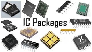
Through-Hole Packaging
Interactive Audio Lesson
Listen to a student-teacher conversation explaining the topic in a relatable way.
Introduction to Through-Hole Packaging
🔒 Unlock Audio Lesson
Sign up and enroll to listen to this audio lesson

Today, we're exploring through-hole packaging. Can anyone tell me what distinguishes this packaging type from others, like surface-mount technology?

Isn't it about the long leads that go through holes in the PCB?
Exactly! Through-hole packaging features long metal leads. These are inserted into the PCB and soldered on the opposite side, making them quite durable. Remember: 'Long Leads = Strong Connections' can be a good way to remember it.

Why would we choose this type over surface-mount?
Great question! Let's explore that in detail. This type is particularly strong mechanically, making it suitable for high-vibration applications.

So it’s used in things like power supplies?
Correct! That's one of its primary applications. Now, let's summarize: through-hole packaging is strong, mechanically robust, and great for repairs.
Advantages and Disadvantages
🔒 Unlock Audio Lesson
Sign up and enroll to listen to this audio lesson

We've mentioned some advantages. Can anyone list them?

It’s durable and easy to solder manually, right?
Absolutely! Its *durability* makes it ideal for high-stress environments, and *manual soldering* is easier, perfect for prototyping. But what are some drawbacks?
I think the size is a problem; it takes more space on the board.
Exactly! Larger size leads to reduced component density. Plus, it's slower to assemble compared to surface-mount technology. Keep in mind: 'Big and Slower' sums up its disadvantages.
So it's more costly in high volumes too?
You're right! Let's summarize: the advantages are mechanical strength and repairability, while disadvantages include size and costs.
Applications of Through-Hole Packaging
🔒 Unlock Audio Lesson
Sign up and enroll to listen to this audio lesson
Let's move on to applications. Where do we typically see through-hole packaging used?
In high-current applications, maybe?
Yes, exactly! It’s commonly used in power electronics that require high current, like power supplies. Anyone else?
Military and aerospace?
Absolutely! They value reliability and robustness. So, to sum up: through-hole packaging is used in high-current electronics, prototyping, and critical applications like military.
Introduction & Overview
Read summaries of the section's main ideas at different levels of detail.
Quick Overview
Standard
Through-hole packaging features long metal leads inserted into holes on a PCB, offering mechanical durability and ease of repair. Although larger than other types, it is ideal for high-stress applications, military use, and prototyping; however, it suffers from slower assembly and higher costs in mass production.
Detailed
Through-Hole Packaging
Through-hole packaging is a traditional method for mounting electronic components on printed circuit boards (PCBs). This approach involves inserting long metal leads of components through drilled holes in the PCB and soldering them on the opposite side. It is especially beneficial in applications that require high mechanical strength or facilitate easy repairs.
Design Features
- Long Component Leads: These leads pass through the PCB, providing robust anchoring.
- Large Size: Through-hole components are bulkier than surface-mount components, requiring more space.
- Higher Profile: The components have greater vertical dimensions, impacting PCB layout.
Advantages
- Mechanical Durability: These components provide robust support in high-vibration environments, making them suitable for demanding applications.
- Ease of Manual Soldering: They are user-friendly for manual soldering, benefiting prototyping and low-volume production.
- Repairability: Their visible leads allow for straightforward repair in case of malfunctions.
Disadvantages
- Larger Size: This design limits the density of components on a PCB.
- Slower Assembly Process: The manual handling contributes to a slower assembly process compared to surface-mount technology (SMT).
- Higher Cost for High Volumes: The complexities in assembly can lead to increased costs in mass manufacturing.
Applications
Through-hole packaging is commonly employed in:
- High-Current Applications: Found in power electronics requiring stability, such as power supplies.
- Prototype and Low-Volume Production: Used where flexibility in design and easy soldering is essential.
- Military and Aerospace: Ideal where reliability is paramount, as in military and aerospace electronics.
Youtube Videos

Audio Book
Dive deep into the subject with an immersive audiobook experience.
Definition and Overview of Through-Hole Packaging
Chapter 1 of 5
🔒 Unlock Audio Chapter
Sign up and enroll to access the full audio experience
Chapter Content
Through-hole packaging was the standard in the early days of semiconductor packaging. In this method, components have long leads that are inserted into holes drilled through the PCB and soldered on the opposite side. This type of packaging is widely used in applications requiring high mechanical strength or easy repairability.
Detailed Explanation
Through-hole packaging refers to a traditional method of connecting electronic components to printed circuit boards (PCBs). This method involves placing components with elongated metal leads through holes in the PCB, which are then soldered from the other side. This design is beneficial for applications needing components that can withstand mechanical stress and can be easily repaired, making it ideal for certain industries. As a result, through-hole packaging has gained prominence in early electronics but continues to have specific applications even today.
Examples & Analogies
Imagine building a treehouse where you use long screws that go all the way through the wood to secure the structure together. Just like those screws allow you to repair or modify the treehouse easily, through-hole packaging allows engineers to replace or fix components on a circuit board more readily.
Design Features of Through-Hole Packaging
Chapter 2 of 5
🔒 Unlock Audio Chapter
Sign up and enroll to access the full audio experience
Chapter Content
● Long Component Leads: Components have long metal leads that pass through the PCB and are soldered on the opposite side.
● Large Size: Through-hole components are typically larger and bulkier compared to surface-mount counterparts.
● Higher Profile: The height of the component is greater, leading to larger vertical dimensions on the PCB.
Detailed Explanation
The design features of through-hole packaging include several distinct characteristics. First, the components have long leads, allowing them to be inserted into the PCB. Second, these components are generally larger and bulkier compared to their surface-mounted equivalents. Finally, the height of these components is greater, which means they occupy more vertical space on the PCB. This higher profile can limit the overall compactness of the circuit board.
Examples & Analogies
Think of it like a traditional lamp with a long power cord that needs to fit through a hole in a table to connect to the wall. Just like that lamp takes up more space on the table and protrudes higher due to its long design, through-hole components occupy more room and extend higher on the PCB compared to smaller, flat surface-mounted devices.
Advantages of Through-Hole Packaging
Chapter 3 of 5
🔒 Unlock Audio Chapter
Sign up and enroll to access the full audio experience
Chapter Content
● Mechanical Durability: Through-hole components are more mechanically robust, making them suitable for high-vibration environments or high-stress applications.
● Ease of Manual Soldering: Through-hole packages are easier to solder manually, making them ideal for low-volume or prototyping applications.
● Repairability: Components can be more easily replaced or repaired in the event of failure, as their leads are visible.
Detailed Explanation
Through-hole packaging offers several advantages primarily due to its robust design. Firstly, these components can endure physically demanding situations, such as significant vibrations or mechanical stress, which makes them a reliable choice for certain applications. Secondly, they are easier for engineers to solder manually, thus making through-hole components favorable in prototyping or small-scale production settings. Lastly, their design allows for straightforward replacement or repair since the leads are accessible and visible on the board.
Examples & Analogies
Imagine how some cars are designed to perform better on bumpy roads because they have stronger suspensions and heavier components. Similarly, through-hole components are built to be tougher in high-stress environments, which is why they're often chosen for situations where reliability is crucial.
Disadvantages of Through-Hole Packaging
Chapter 4 of 5
🔒 Unlock Audio Chapter
Sign up and enroll to access the full audio experience
Chapter Content
● Larger Size: Through-hole packages take up more space on the PCB, reducing the overall component density and increasing board size.
● Slower Assembly Process: The assembly process for through-hole packages is slower compared to surface-mount technology, especially in automated manufacturing.
● Higher Cost for High Volumes: Through-hole packages are generally more expensive to manufacture in high volumes due to the more complex assembly process.
Detailed Explanation
While through-hole packaging has significant advantages, it also comes with drawbacks. Being larger and bulkier, these components reduce the overall density of parts on a PCB, often necessitating larger boards. The assembly of through-hole packages is meticulous and takes longer compared to surface-mount technology, leading to increased production times. Moreover, assembling these components is generally more costly in high-volume scenarios due to the intricacies involved in the process.
Examples & Analogies
Consider packing suitcases for a family vacation. If you have bulky clothing instead of compact outfits, your suitcase takes up more space and is harder to carry. Similarly, through-hole components take more room on a PCB and can slow down production just like packing bulky clothes can slow down your travel plans.
Applications of Through-Hole Packaging
Chapter 5 of 5
🔒 Unlock Audio Chapter
Sign up and enroll to access the full audio experience
Chapter Content
● High-Current Applications: Used in power electronics where high current handling and mechanical stability are required, such as in power supplies and power transistors.
● Prototype and Low-Volume Production: Ideal for prototyping, repair, and small-run production where ease of hand-soldering and flexibility are key.
● Military and Aerospace: Often used in applications where reliability and robustness are critical, such as in aerospace or military electronics.
Detailed Explanation
Through-hole packaging finds its place in various specialized applications. It is particularly suited for high-current electronics, where durability is essential, such as power supplies. Additionally, through-hole components are commonly used in prototyping environments and low-volume production due to their manual soldering capability. Lastly, there is a strong reliance on through-hole packaging in military and aerospace industries, where the dependability of electronic components is non-negotiable.
Examples & Analogies
Think of through-hole packaging like the sturdy parts of a rescue vehicle—it's vital that every component holds up under pressure. Just as firefighters need reliable gear in emergencies, certain industries depend on the robust attributes of through-hole components to ensure mission success.
Key Concepts
-
Long Leads: These allow components to be inserted into the PCB, providing greater mechanical strength.
-
Ease of Manual Soldering: Simplifies prototyping and repair processes.
-
Mechanical Durability: Essential for high-stress and military applications.
-
Larger Component Size: Ensure lower component density on the PCB.
Examples & Applications
Power supplies often employ through-hole components for their ability to handle high current and provide robust performance.
In prototyping, engineers frequently choose through-hole packaging for its ease of manual soldering and flexibility.
Memory Aids
Interactive tools to help you remember key concepts
Rhymes
For strength and repair, through-holes do care!
Stories
Once upon a time in a rugged workshop, through-hole components stood tall, ready to face heavy currents and be repaired effortlessly.
Memory Tools
Remember 'LERM': Leads, Ease of repair, Robustness, Manual soldering for through-holes.
Acronyms
THP
Through-hole
High strength
Prototyping.
Flash Cards
Glossary
- ThroughHole Packaging
A packaging method where components are mounted on circuit boards using long leads inserted into drilled holes.
- Mechanical Strength
The ability of a component to withstand stress and vibration.
- Soldering
A process of joining electronic components to a PCB using a melted metal alloy.
- Prototyping
The process of developing a preliminary model of a product to test concepts.
- PCB (Printed Circuit Board)
A board used for physically supporting and connecting electronic components.
Reference links
Supplementary resources to enhance your learning experience.