
Comparative Summary of Techniques
Enroll to start learning
You’ve not yet enrolled in this course. Please enroll for free to listen to audio lessons, classroom podcasts and take practice test.
Interactive Audio Lesson
Listen to a student-teacher conversation explaining the topic in a relatable way.
Bulk Micromachining
🔒 Unlock Audio Lesson
Sign up and enroll to listen to this audio lesson

Let's discuss bulk micromachining first. This technique involves the selective removal of material from a silicon wafer. Can anyone tell me what types of structures are created using this method?

Are they things like cavities and pressure sensors?
Exactly! Bulk micromachining is great for creating features like cavities and membranes. Now, what do you think are some strengths of this method?

It must have high mechanical strength since it uses the bulk of the wafer.
Correct! The bulk substrate allows for strong structures. But what about its limitations?

Maybe controlling the depth of the etching is hard?
Yes, depth control can be challenging. Remember this as a key point: 'Depth control is difficult.'
In summary, bulk micromachining creates strong microstructures but struggles with precision.
Surface Micromachining
🔒 Unlock Audio Lesson
Sign up and enroll to listen to this audio lesson

Now let’s move to surface micromachining. Unlike bulk methods, this creates structures layer by layer on the surface. Can anyone describe the typical materials used?

I think polysilicon is one of the materials.
Correct! Polysilicon is used as a structural layer, along with silicon nitride. What structures can we build using this technique?
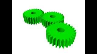
Beams and micro gears?
Perfect! And what’s a significant advantage of this method?
It allows for more complex structures!
Yes! The complexity and integration potential with electronic components are crucial highlights of surface micromachining.
To recap, surface micromachining provides flexibility in design but has limitations with structural thickness.
High-Aspect-Ratio Micromachining
🔒 Unlock Audio Lesson
Sign up and enroll to listen to this audio lesson
Shifting gears, let's dive into High-Aspect-Ratio Micromachining or HARMS. Who knows what technologies are used in this method?
LIGA and DRIE are part of it, right?
Absolutely! HARMS uses advanced methods for precise microstructure fabrication. What do we create with this technique?
Tall and narrow microstructures!
Exactly. These are crucial for applications like microturbines. Now, let’s talk about the advantages.
It produces deep and precise parts.
Yes! However, what might be some drawbacks?
It can be more expensive to implement?
Yes, that's correct! In summary, HARMS is valuable for its precision but carries costs.
Wafer Bonding
🔒 Unlock Audio Lesson
Sign up and enroll to listen to this audio lesson
Wafer bonding is essential for creating multi-layered MEMS devices. Can anyone name the bonding methods?
Anodic bonding and fusion bonding?
That's right! Anodic bonding joins silicon to glass, while fusion bonding is silicon-to-silicon. What's the main purpose of wafer bonding?
To seal cavities and stack layers?
Exactly! This allows for compact design. But what could be a potential limitation?
Defects during bonding could occur?
Right again! Summary: wafer bonding enables multi-layer functionalities but is susceptible to defects.
Introduction & Overview
Read summaries of the section's main ideas at different levels of detail.
Quick Overview
Standard
The comparative summary of techniques outlines the major MEMS fabrication methods, including bulk micromachining, surface micromachining, HARMS, wafer bonding, soft lithography, and additive micromanufacturing. It highlights key materials, typical applications, strengths, and limitations of each technique, aiding in understanding their suitability for specific applications.
Detailed
Comparative Summary of Techniques
In MEMS fabrication, different techniques offer unique benefits and drawbacks, which are crucial in choosing the appropriate method for a specific application. This section outlines the primary MEMS fabrication methodologies, comparing their processes, materials, strengths, and limitations as follows:
1. Bulk Micromachining
- Process: Selective removal of material from a silicon wafer.
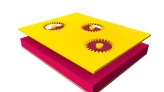
- Structures: Cavities, membranes, and pressure sensor housings.
- Strengths: High mechanical strength due to the utilization of bulk substrate.
- Limitations: Difficulty in controlling depth precision.
2. Surface Micromachining
- Process: Layered deposition on the substrate surface.
- Structures: Beams, gears, and actuators.
- Strengths: Complex structures can be built with potential integration into CMOS electronics.
- Limitations: Limited structural thickness control due to the deposition method.
3. High-Aspect-Ratio Micromachining (HARMS)
- Process: Combines technologies like LIGA and DRIE for precise microstructure fabrication.
- Structures: Tall and narrow components.
- Strengths: Ability to create complex geometries with deep structures.
- Limitations: Higher costs associated with the processes.
4. Wafer Bonding
- Process: Joining silicon with various materials under various conditions.
- Structures: Multi-layered MEMS devices and sealed cavities.
- Strengths: Enables compact and multi-functional designs.
- Limitations: Prone to defects due to bonding errors.
5. Soft Lithography and Polymer MEMS
- Process: Uses polymers for flexible biocompatible structures.
- Structures: Various soft MEMS elements.
- Strengths: Low-cost fabrication with biocompatibility.
- Limitations: Mechanical rigidity challenges.
6. Additive Micromanufacturing
- Process: 3D printing techniques for MEMS.
- Structures: Custom micro-geometries.
- Strengths: High design flexibility and rapid prototyping abilities.
- Limitations: Limited by material capabilities and resolution.
Understanding these techniques allows for informed decisions in MEMS design and engineering, ultimately contributing to improved device functionality.
Youtube Videos
Audio Book
Dive deep into the subject with an immersive audiobook experience.
Bulk Micromachining
Chapter 1 of 6
🔒 Unlock Audio Chapter
Sign up and enroll to access the full audio experience
Chapter Content
Fabrication Technique: Bulk Micromachining
Key Process: Etching
Typical Structures: Cavities, membranes
Material Strengths: High mechanical strength
Limitations: Depth control is difficult
Detailed Explanation
Bulk micromachining is a fabrication technique that primarily focuses on etching away material from a silicon wafer to create structures like cavities and membranes. This process provides high mechanical strength, making it suitable for applications where robust structures are needed. However, one of the significant challenges with bulk micromachining is that controlling the etching depth can be quite difficult, which may affect the precision of the fabricated structures.
Examples & Analogies
Think of bulk micromachining like sculpting a statue from a block of marble. While you can create strong, detailed sculptures, it can be challenging to remove just the right amount of material without going too deep or leaving rough edges.
Surface Micromachining
Chapter 2 of 6
🔒 Unlock Audio Chapter
Sign up and enroll to access the full audio experience
Chapter Content
Fabrication Technique: Surface Micromachining
Key Process: Layered deposition
Typical Structures: Beams, gears, actuators
Material Strengths: CMOS integration possible
Limitations: Structure thickness is limited
Detailed Explanation
Surface micromachining is a fabrication approach that constructs microstructures layer by layer directly on the surface of a substrate, like silicon. This technique allows for the creation of complex devices such as beams, gears, and actuators. A notable advantage is the ability to integrate these components with CMOS technology, enhancing performance. However, a limitation arises due to the restricted thickness of the structures that can be deposited, which can affect device functionality.
Examples & Analogies
Imagine layering paper to create a multi-layered cake. You can decorate each layer and make it complex and interesting, but the size of each layer (or paper) is limited, which can restrict how tall or elaborate your cake can be.
High-Aspect-Ratio Micromachining (HARMS)
Chapter 3 of 6
🔒 Unlock Audio Chapter
Sign up and enroll to access the full audio experience
Chapter Content
Fabrication Technique: HARMS (e.g., LIGA, DRIE)
Key Process: X-ray lithography
Typical Structures: High aspect ratio parts
Material Strengths: Deep and precise structures
Limitations: Expensive and complex
Detailed Explanation
High-Aspect-Ratio Micromachining (HARMS) includes advanced techniques such as LIGA and Deep Reactive Ion Etching (DRIE) to create tall, narrow structures. These processes involve cutting-edge methods such as X-ray lithography, resulting in high precision and creating intricate designs. However, the major drawback is the expense and complexity involved in these methods, which may not be feasible for all applications.
Examples & Analogies
Think of HARMS like designing and constructing skyscrapers. They need deeply technical planning and heavy investments, but the result is clear: tall, impressive structures that can host a variety of functions and services. Not everyone can afford to build a skyscraper due to these challenges.
Wafer Bonding
Chapter 4 of 6
🔒 Unlock Audio Chapter
Sign up and enroll to access the full audio experience
Chapter Content
Fabrication Technique: Wafer Bonding
Key Process: Sealing and stacking
Typical Structures: Enclosed cavities
Material Strengths: Enables multi-layered MEMS
Limitations: Bonding defects may occur
Detailed Explanation
Wafer bonding is a critical process in MEMS fabrication, allowing for the creation of multi-layered devices by sealing or stacking different layers together. This technique is useful for constructing enclosed cavities which are essential for many MEMS applications. While wafer bonding enables enhanced device functionality through multi-layer integration, it is susceptible to defects that can arise during the bonding process, posing challenges for yield and reliability.
Examples & Analogies
Imagine putting together a multi-layered sandwich. Each layer adds more flavor and texture, but if the ingredients aren’t stacked well or there’s an issue with the glue (like mayonnaise), parts can fall apart or not hold together properly, making the whole sandwich less satisfying.
Soft Lithography
Chapter 5 of 6
🔒 Unlock Audio Chapter
Sign up and enroll to access the full audio experience
Chapter Content
Fabrication Technique: Soft Lithography
Key Process: Polymer casting
Typical Structures: Flexible bio-MEMS
Material Strengths: Low-cost, biocompatible
Limitations: Low mechanical rigidity
Detailed Explanation
Soft lithography utilizes polymers to create flexible and bio-compatible MEMS structures through casting techniques. It is a cost-effective method that can yield structures that are suitable for biomedical applications. However, the downside is that the resulting structures tend to have lower mechanical rigidity compared to those made from silicon or other stronger materials, which can limit their use in certain applications.
Examples & Analogies
Think of soft lithography like creating a mold for chocolate candies using flexible silicone molds. It’s cheaper, and the candies can have fun shapes and decorations, but the molds themselves can be too soft to withstand extreme heat or pressure, limiting what you can use them for.
Additive Micromanufacturing
Chapter 6 of 6
🔒 Unlock Audio Chapter
Sign up and enroll to access the full audio experience
Chapter Content
Fabrication Technique: Additive Micromanufacturing
Key Process: 3D printing techniques
Typical Structures: Custom micro-geometries
Material Strengths: Rapid prototyping
Limitations: Limited by material resolution
Detailed Explanation
Additive micromanufacturing refers to techniques like 3D printing, offering significant flexibility in design and the ability to create complex geometries rapidly. While it allows for extensive customization and is ideal for prototyping new ideas, the process can be limited by the resolution of the chosen materials, meaning the finished product may not always meet the desired precision.
Examples & Analogies
Imagine bringing a plastic toy figure to life using a 3D printer. You can customize it to your heart's desire, but if the printer has a low resolution, the figure might end up looking rough or imprecise, like a toy with fuzzy features or rough edges—great for quick trials, but not perfect for store shelves.
Key Concepts
-
Bulk Micromachining: A technique that creates structures by etching into the silicon wafer.
-
Surface Micromachining: A layered approach to building complex microstructures.
-
HARMS: Utilizes specific techniques for fabricating high aspect ratio structures.
-
Wafer Bonding: Essential for creating multi-layered devices.
-
Soft Lithography: Focused on flexible and low-cost polymer MEMS.
-
Additive Micromanufacturing: Allows for custom fabrication and rapid prototyping.
Examples & Applications
Bulk micromachining applications include pressure sensors and accelerometers.
Surface micromachining examples include RF MEMS switches and micro mirrors.
HARMS is used to fabricate microfluidic channels and biomedical implants.
Wafer bonding techniques create multi-layered devices for enhanced functionality.
Soft lithography is applied in developing lab-on-chip systems and wearable health monitors.
Memory Aids
Interactive tools to help you remember key concepts
Rhymes
Bulk's got the strength, but depth's a test, Surface layers bring complexity, that's the best.
Stories
Imagine a factory where each floor builds layers of different materials. The bottom layer is strong (bulk micromachining), but the upper layers are more intricate and flexible (surface micromachining).
Memory Tools
Remember 'B-S-H-W-S-A' for Bulk, Surface, High Aspect Ratio, Wafer bonding, Soft lithography, Additive to recall all techniques.
Acronyms
Use 'B-S-H-W-S-A' to memorize different MEMS fabrication techniques
Bulk
Surface
HARMS
Wafer bonding
Soft lithography
Additive.
Flash Cards
Glossary
- Bulk Micromachining
A MEMS fabrication technique that selectively removes material from a substrate to create structures.
- Surface Micromachining
A fabrication method where microstructures are built layer by layer on the surface of a substrate.
- HighAspectRatio Micromachining (HARMS)
A method that produces tall and narrow microstructures using advanced lithography and etching techniques.
- Wafer Bonding
A process of joining two separate wafers or materials to create a composite structure.
- Soft Lithography
A technique for fabricating microstructures using flexible molds or stamps.
- Additive Micromanufacturing
An emerging method involving adding material layer-by-layer, such as through 3D printing.
Reference links
Supplementary resources to enhance your learning experience.