
Process Features - 5.2.1
Enroll to start learning
You’ve not yet enrolled in this course. Please enroll for free to listen to audio lessons, classroom podcasts and take practice test.
Interactive Audio Lesson
Listen to a student-teacher conversation explaining the topic in a relatable way.
Introduction to Bulk Micromachining
🔒 Unlock Audio Lesson
Sign up and enroll to listen to this audio lesson

Welcome, class! Today, we're diving into the exciting world of bulk micromachining. Can anyone share what they think bulk micromachining involves?

Isn't it about removing material from silicon wafers to create microstructures?
Exactly! Bulk micromachining is the selective removal of material, often used to produce complex structures on silicon wafers. Can anyone list some structures that can be created?

Cavities and membranes?
Great job! We can create diaphragms and pressure sensor housings too. Remember the acronym 'DCP' — it stands for Diaphragms, Cavities, and Pressure housings. Let's keep that in mind!
Etching Techniques in Bulk Micromachining
🔒 Unlock Audio Lesson
Sign up and enroll to listen to this audio lesson

Now, let's talk about the etching techniques used in bulk micromachining. Who can tell me the difference between wet and dry etching?

Wet etching uses chemicals to dissolve silicon, while dry etching uses plasma?
Right! Wet etching often leads to anisotropic etching with angled sides, while dry etching, like RIE or DRIE, offers greater control and allows for vertical walls. Can anyone remember what 'RIE' stands for?

It’s Reactive Ion Etching!
Correct! Keeping these etching techniques in mind helps us understand how we design our microstructures.
Could you give an example when we’d use one over the other?
Definitely! We would use wet etching for less precision where costs are a concern, while dry etching is preferred for high-precision applications. Great questions, everyone!
Applications of Bulk Micromachining
🔒 Unlock Audio Lesson
Sign up and enroll to listen to this audio lesson
Let's now discuss some applications. Can anyone think of where we use devices made with bulk micromachining?
Pressure sensors?
Yes! Bulk micromachined pressure sensors are widely used in various industries. Can someone give me another example?
Accelerometers are another example!
Exactly! These sensors are crucial in many consumer electronics as they detect motion. Remember, every application stems from the unique features of the processes. Underlining their significance helps us in the future!
How does that tie into other MEMS applications?
Great follow-up! These applications feed into a larger ecosystem of MEMS technologies that contribute to automation and smart devices.
Key Takeaways
🔒 Unlock Audio Lesson
Sign up and enroll to listen to this audio lesson
Before we wrap up, what are the key points we discussed regarding bulk micromachining?
We talked about how bulk micromachining removes material to create various structures!
And the etching techniques, both wet and dry!
Exactly! Remember the applications like pressure sensors and accelerometers. This solid understanding of the process features will be key for your future studies in MEMS. Great session, everyone!
Introduction & Overview
Read summaries of the section's main ideas at different levels of detail.
Quick Overview
Standard
Bulk micromachining is a critical fabrication technique in MEMS, where material is selectively removed from silicon wafers to construct various structures. Key processes include wet and dry etching techniques, which allow for the creation of precise microcomponents such as pressure sensors and diaphragms.
Detailed
Process Features in Bulk Micromachining
Bulk micromachining is a significant technique within MEMS (Micro-Electro-Mechanical Systems) fabrication, involving the selective removal of material from a silicon wafer to create desired structures. This section focuses on several key features:
Structures Created
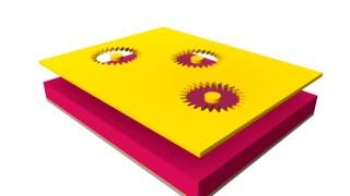
- Cavities: Hollow spaces formed within the silicon wafer.
- Diaphragms and Membranes: Thin flexible components used in pressure sensing and other applications.
- Sensor Housings: Structures that protect and enclose sensitive sensor elements.
Wafer Utilization
- The entire bulk of the silicon wafer serves as the structural base for these microcomponents, providing inherent structural strength.
Etching Techniques
- Wet Etching: Utilizes chemical solutions such as KOH and TMAH. It is characterized by anisotropic etching, leading to angled sidewalls that depend on crystal orientation.
- Dry Etching: Incorporates plasma-based methods like Reactive Ion Etching (RIE) and Deep Reactive Ion Etching (DRIE), which provide greater precision and produce vertical sidewalls.
Applications
- Pressure Sensors: Devices that measure pressure changes through diaphragm movement.
- Accelerometers: Sensors that detect changes in acceleration, vital for various applications including consumer electronics.
- Micromechanical Diaphragms: Used in different sensor applications where flexibility and response time are critical.
Overall, mastering the process features of bulk micromachining is essential for advancing microfabrication techniques and applications in MEMS technology.
Youtube Videos
Audio Book
Dive deep into the subject with an immersive audiobook experience.
Created Structures
Chapter 1 of 6
🔒 Unlock Audio Chapter
Sign up and enroll to access the full audio experience
Chapter Content
Structures such as cavities, diaphragms, membranes, and pressure sensor housings are created.
Detailed Explanation
In bulk micromachining, the fabrication process involves removing material from a silicon wafer to create specific structures. These structures can vary widely in form, including cavities (hollow spaces), diaphragms (thin membranes that can flex), and pressure sensor housings (enclosures for sensors). Each structure serves particular purposes in microelectromechanical systems (MEMS), such as sensing pressure variations or acting as mechanical supports.
Examples & Analogies
Imagine sculpting a piece of wood by carefully carving out certain areas. Just as a sculptor removes wood to create a statue or a useful item, engineers use bulk micromachining to carve out features in silicon to make devices like pressure sensors that could help in applications such as weather monitoring.
Utilization of the Wafer Bulk
Chapter 2 of 6
🔒 Unlock Audio Chapter
Sign up and enroll to access the full audio experience
Chapter Content
The entire wafer bulk is used as the structural base.
Detailed Explanation
Bulk micromachining takes advantage of the whole silicon wafer, using the material itself as the foundation for the microstructures being formed. This is different from other methods that might only apply coatings or layers on top of a substrate. The structural base formed by the wafer provides strength and stability, which is essential for the performance of MEMS devices.
Examples & Analogies
Think of a construction site where a building uses concrete pillars. The concrete forms the main structure that can hold additional materials and features on top of it. Similarly, in bulk micromachining, the silicon wafer acts as the foundational structure upon which other elements can be added or modified.
Etching Techniques: Overview
Chapter 3 of 6
🔒 Unlock Audio Chapter
Sign up and enroll to access the full audio experience
Chapter Content
Etching Techniques:
Detailed Explanation
Etching is a critical process in bulk micromachining used to remove material from the silicon wafer to create desired features. There are two main types of etching techniques employed: wet etching and dry etching. Both methods have their own advantages and are chosen based on the specific requirements of the structure being fabricated.
Examples & Analogies
Imagine you are carving designs into a pumpkin. You can use a spoon (wet etching) to scoop out large areas quickly or a small knife (dry etching) to carefully cut precise lines and shapes. Depending on the design you want to achieve, you would choose the tool that gives you the best results.
Wet Etching Process
Chapter 4 of 6
🔒 Unlock Audio Chapter
Sign up and enroll to access the full audio experience
Chapter Content
Wet Etching:
- Uses chemical solutions (e.g., KOH, TMAH) to dissolve silicon along specific crystal planes.
- Results in anisotropic (direction-dependent) etching with characteristic angled sidewalls.
Detailed Explanation
Wet etching involves immersing the silicon wafer in a chemical solution that selectively dissolves silicon. This process follows the crystal structure of silicon, leading to etching that can create angled sidewalls and specific features. Wet etching is valued for its simplicity and the ability to etch deep structures, but it can be less precise than dry etching when it comes to feature size.
Examples & Analogies
Consider how water can carve valleys in a landscape. When water flows along a certain path, it erodes the earth in a way that follows the contours of the landscape. Similarly, in wet etching, the chemical solution follows the silicon’s crystal structure to create precise etches in specific directions.
Dry Etching Techniques
Chapter 5 of 6
🔒 Unlock Audio Chapter
Sign up and enroll to access the full audio experience
Chapter Content
Dry Etching:
- Uses plasma-based techniques such as Reactive Ion Etching (RIE) or Deep Reactive Ion Etching (DRIE) for greater precision and vertical sidewalls.
Detailed Explanation
Dry etching uses plasma technology to remove silicon and create more defined features. Techniques like Reactive Ion Etching (RIE) and Deep Reactive Ion Etching (DRIE) allow for greater control over the etching process. This leads to vertical sidewalls, making it ideal for producing features that require tight tolerances and complexities that cannot be achieved with wet etching.
Examples & Analogies
Think of a laser cutter that can cut through materials with high precision, allowing for complex designs and shapes. Dry etching works similarly, using plasma to etch the silicon wafer with high accuracy, creating intricate details that are crucial in MEMS device performance.
Applications of Bulk Micromachining
Chapter 6 of 6
🔒 Unlock Audio Chapter
Sign up and enroll to access the full audio experience
Chapter Content
Applications:
- Pressure sensors
- Accelerometers
- Micromechanical diaphragms
Detailed Explanation
Bulk micromachining is applied in various critical areas. Pressure sensors use it to sense changes in pressure accurately, while accelerometers measure acceleration forces, essential in devices like smartphones. Micromechanical diaphragms are used in applications like microphones where sound waves create a pressure difference that the diaphragm feels, translating those waves into electrical signals.
Examples & Analogies
Consider how a car uses various sensors to monitor its operation. Just as a car's pressure sensors help ensure the tires are inflated correctly, MEMS pressure sensors made through bulk micromachining help monitor conditions in numerous technologies, from consumer electronics to aerospace.
Key Concepts
-
Bulk Micromachining: The process of removing material from silicon wafers to create structures.
-
Wet Etching: Chemical removal of silicon yielding angled sidewalls.
-
Dry Etching: Plasma-based etching providing vertical sidewalls and higher precision.
-
Applications: Use of structures for sensors like pressure sensors and accelerometers.
Examples & Applications
In the manufacture of pressure sensors, diaphragms are created using bulk micromachining.
Accelerometers are developed by creating cavities and structural layers in silicon wafers.
Memory Aids
Interactive tools to help you remember key concepts
Rhymes
Etch, etch, what do we see? Angled walls and cavities, that's the key!
Stories
Once upon a time in a fab lab, a scientist wished to create tiny machines. With silicon wafers and etching tools, they sculpted sensors and switches, making dreams come true!
Memory Tools
Remember 'WDC' for Wet etching, Dry etching, and Cavities!
Acronyms
Use the acronym 'DSM' to recall 'Diaphragms, Sensors, and Micromachining'.
Flash Cards
Glossary
- Bulk Micromachining
A fabrication process that involves the selective removal of material from a silicon wafer to create mechanical structures.
- Wet Etching
An etching process that uses chemical solutions to dissolve silicon along specific crystal planes, resulting in angled sidewalls.
- Dry Etching
An etching process that uses plasma techniques for high precision including Reactive Ion Etching (RIE) and Deep Reactive Ion Etching (DRIE).
- Cavities
Hollow structures created within the silicon wafer.
- Diaphragms
Flexible membranes used in pressure sensors and other applications.
Reference links
Supplementary resources to enhance your learning experience.