
Fabrication Techniques – Bulk Micromachining, Surface Micromachining, and More
Enroll to start learning
You’ve not yet enrolled in this course. Please enroll for free to listen to audio lessons, classroom podcasts and take practice test.
Interactive Audio Lesson
Listen to a student-teacher conversation explaining the topic in a relatable way.
Introduction to MEMS Fabrication Techniques
🔒 Unlock Audio Lesson
Sign up and enroll to listen to this audio lesson

Welcome class! Today we're diving into MEMS fabrication techniques. Can anyone tell me what MEMS stands for?

I think it stands for Micro-Electromechanical Systems.
Exactly! MEMS involve tiny mechanical and electrical components. We'll start with bulk micromachining. What do you think this technique involves?

Maybe it has something to do with removing material from a solid piece?
Correct! Bulk micromachining selectively removes material from a silicon wafer to create structures. Now, can anyone name some structures that can be formed using this method?

How about pressure sensors or membranes?
Great examples! Remember that these structures are crucial for various applications. Let's move on to wet and dry etching techniques.

What's the difference between them?
Wet etching uses chemicals, while dry etching involves plasma. Dry etching offers better precision, leading to vertical walls. Always think 'wet for basic, dry for precision!'
Surface Micromachining Techniques
🔒 Unlock Audio Lesson
Sign up and enroll to listen to this audio lesson

Next, let's discuss surface micromachining. Who can explain how it differs from bulk micromachining?
Isn't it about building structures on the layer of a substrate instead of cutting into it?
Exactly! Surface micromachining adds layers instead of removing material. What materials do you think are commonly used?
I remember polysilicon and silicon dioxide from our last class.
Spot on! These materials allow creating movable parts once sacrificial layers are removed. What are some applications of this technology?
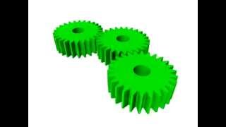
Micro gears and RF switches?
Yes! They are great examples. To help you remember, think of 'Surface = Layers, Flexibility, Integration!'
High-Aspect-Ratio Micromachining (HARMS)
🔒 Unlock Audio Lesson
Sign up and enroll to listen to this audio lesson
Now, let’s explore high-aspect-ratio micromachining, or HARMS. Why do you think this is important?
Maybe for creating tall microstructures?
Exactly right! HARMS techniques, like LIGA, are vital for producing high-precision components. Can someone summarize how LIGA works?
It combines X-ray lithography and molding, right?
Correct! And this leads to applications in biomedical implants and microfluidic channels. Remember: 'HARMS = Height and Precision!'
Wafer Bonding and Soft Lithography
🔒 Unlock Audio Lesson
Sign up and enroll to listen to this audio lesson
Finally, we have wafer bonding and soft lithography. Can anyone provide a brief description of wafer bonding?
It's a method to join different materials together, right?
Yes! Techniques include anodic and fusion bonding. They play a key role in creating layered MEMS. What about soft lithography? Any insights?
That uses polymers like PDMS for flexible devices?
Great job! This method is ideal for creating bio-compatible structures. Just remember, 'Wafer Bonding = Joining Materials; Soft Lithography = Flexibility!'
Introduction & Overview
Read summaries of the section's main ideas at different levels of detail.
Quick Overview
Standard
An exploration of critical fabrication techniques in MEMS, this section delves into bulk and surface micromachining processes, their features, applications, and advantages. Innovations such as wafer bonding and soft lithography are also discussed, highlighting their roles in modern microsystems.
Detailed
Detailed Summary
This section focuses on various fabrication techniques crucial for Micro-Electromechanical Systems (MEMS), which involve precise processes for constructing micro-scale mechanical and electrical components, primarily on silicon substrates. The techniques discussed are:
1. Bulk Micromachining
This involves the selective removal of material from a silicon wafer to create structures. The methods include:
- Wet Etching (using chemical solutions like KOH) leads to anisotropic etching.
- Dry Etching (using plasma techniques) provides better precision.
Applications include pressure sensors and accelerometers.
2. Surface Micromachining
This technique builds structures layer by layer, with a focus on deposition processes for structural and sacrificial layers. Common materials include polysilicon and silicon dioxide.
Advantages include the ability to create complex structures and ease of integration with electronic components, with applications in RF MEMS switches and micro gears.
3. High-Aspect-Ratio Micromachining (HARMS)
Used for creating tall, narrow structures. Techniques like LIGA and DRIE are used for producing precise components such as microturbines and biomedical implants.
4. Wafer Bonding
Essential for multi-layer MEMS, this process includes various bonding methods (anodic, fusion, adhesive), with applications in packaging and integration of components.
5. Soft Lithography and Polymer MEMS
These techniques involve flexible polymer materials to create structures, offering advantages in biocompatibility for applications like lab-on-chip systems.
All these methods provide essential tools for advanced fabrication in MEMS, catering to a variety of material and geometrical needs.
Youtube Videos
Audio Book
Dive deep into the subject with an immersive audiobook experience.
Introduction to MEMS Fabrication
Chapter 1 of 9
🔒 Unlock Audio Chapter
Sign up and enroll to access the full audio experience
Chapter Content
MEMS fabrication involves a series of micro-scale processes that build mechanical and electrical components on substrates, often silicon. These processes are adapted from semiconductor manufacturing but customized to create three-dimensional movable microstructures. This chapter focuses on major MEMS fabrication techniques: bulk micromachining, surface micromachining, and other advanced methods that enable high-performance microsystems.
Detailed Explanation
MEMS, or Micro-Electro-Mechanical Systems, are devices that combine mechanical and electronic components at a micro-scale. The fabrication of these devices involves a series of intricate processes, primarily using materials like silicon. The techniques used in MEMS fabrication originally come from semiconductor manufacturing but are adapted to allow for the creation of complex structures that can move and function at micro-levels. This chapter will discuss the significant techniques such as bulk micromachining and surface micromachining, along with other advanced methods used in producing high-performance microsystems.
Examples & Analogies
Think of MEMS as tiny factories that create incredibly small machines, much like how a car assembly plant makes vehicles. Just as large factories need precise processes to assemble cars, MEMS fabrication requires specialized steps to produce these miniaturized components.
Bulk Micromachining
Chapter 2 of 9
🔒 Unlock Audio Chapter
Sign up and enroll to access the full audio experience
Chapter Content
Bulk micromachining involves the selective removal of material from a silicon wafer to create desired structures, typically by etching deep into the substrate.
● Process Features:
● Structures such as cavities, diaphragms, membranes, and pressure sensor housings are created.
● The entire wafer bulk is used as the structural base.
● Etching Techniques:
● Wet Etching:
○ Uses chemical solutions (e.g., KOH, TMAH) to dissolve silicon along specific crystal planes.
○ Results in anisotropic (direction-dependent) etching with characteristic angled sidewalls.
● Dry Etching:
○ Uses plasma-based techniques such as Reactive Ion Etching (RIE) or Deep Reactive Ion Etching (DRIE) for greater precision and vertical sidewalls.
● Applications:
● Pressure sensors
● Accelerometers
● Micromechanical diaphragms
Detailed Explanation
Bulk micromachining is a technique where material is selectively removed from the bulk of a silicon wafer. This process is critical for creating various structures, such as cavities, membranes, and housing for pressure sensors. There are two primary methods of etching used in bulk micromachining: wet etching and dry etching. Wet etching involves using chemical solutions to dissolve silicon along preferred crystal directions, which creates angled walls. On the other hand, dry etching employs plasma techniques to achieve very precise and vertical structures. These techniques are utilized in applications such as pressure sensors, accelerometers, and mechanical diaphragm systems.
Examples & Analogies
Imagine sculpting a statue from a block of marble. In bulk micromachining, the silicon wafer acts like the marble block, and etching is the sculpting tool that removes excess material to reveal the desired shape, such as a pressure sensor housing.
Surface Micromachining
Chapter 3 of 9
🔒 Unlock Audio Chapter
Sign up and enroll to access the full audio experience
Chapter Content
Surface micromachining builds microstructures layer by layer on the surface of a substrate, rather than etching into the bulk.
● Process Features:
● Involves deposition of structural and sacrificial layers using techniques like LPCVD or sputtering.
● Sacrificial layers are later etched away to release movable parts.
● Typical Materials:
● Structural layers: Polysilicon, silicon nitride
● Sacrificial layers: Silicon dioxide or photoresist
● Advantages:
● Allows more complex structures on a single wafer
● Enables integration with electronic components
● Applications:
● Micro gears and actuators
● RF MEMS switches
● Micromirrors in optical devices
Detailed Explanation
Surface micromachining is a process where microstructures are built on the surface of a substrate, primarily by adding thin films layer by layer. It utilizes deposition methods such as Low-Pressure Chemical Vapor Deposition (LPCVD) or sputtering to create structural and sacrificial layers. Sacrificial layers are temporary materials that support the structural layers during fabrication but are later removed to allow components to move freely. This technique enables the creation of intricate structures that integrate well with electronic components, making it suitable for applications like micro gears, RF MEMS switches, and micromirrors used in optical devices.
Examples & Analogies
Think of surface micromachining like building a layered cake, where each layer represents a part of the microstructure. The structural layers are like the cake layers, and the sacrificial layers are like frosting that holds everything together temporarily until the cake is completed and the frosting is removed.
High-Aspect-Ratio Micromachining (HARMS)
Chapter 4 of 9
🔒 Unlock Audio Chapter
Sign up and enroll to access the full audio experience
Chapter Content
Used when devices require tall and narrow microstructures.
● Techniques Used:
● LIGA Process: Combines deep X-ray lithography, electroplating, and molding.
● Deep Reactive Ion Etching (DRIE): Also known as the Bosch process, capable of producing deep, vertical sidewalls with high precision.
● Applications:
● Microturbines
● Microfluidic channels
● Biomedical implants
Detailed Explanation
High-aspect-ratio micromachining (HARMS) is employed in manufacturing microstructures that are tall and narrow, which is essential for certain applications. The LIGA process integrates deep X-ray lithography, electroplating, and molding to create these structures. Another popular method used is Deep Reactive Ion Etching (DRIE), often referred to as the Bosch process, which produces structures with precise vertical walls. HARMS is critical in applications such as microturbines, microfluidic channels, and biomedical implants, where the shape and aspect ratio play significant roles in functionality.
Examples & Analogies
Consider HARMS like creating a tall, narrow skyscraper in a city. Just as an architect needs specialized techniques to ensure the building is both tall and structurally sound, similarly, HARMS techniques are needed to fabricate tall microstructures that serve precise functions.
Wafer Bonding
Chapter 5 of 9
🔒 Unlock Audio Chapter
Sign up and enroll to access the full audio experience
Chapter Content
Wafer bonding is essential for creating multi-layered MEMS devices or sealing cavities and fluidic channels.
● Bonding Methods:
● Anodic Bonding: Joins silicon to glass under heat and electric field.
● Fusion Bonding: Direct silicon-to-silicon bonding with high surface flatness.
● Adhesive Bonding: Uses polymer adhesives to join different materials.
● Applications:
● Packaging of pressure sensors
● Encapsulation of vacuum cavities
● Integration of microfluidic devices
Detailed Explanation
Wafer bonding is a critical process in MEMS fabrication, allowing the creation of complex, multi-layered devices. The methods of bonding include anodic bonding, which involves heating and applying an electric field to join silicon and glass, fusion bonding, where high-flatness silicon surfaces are directly bonded, and adhesive bonding, which uses polymer materials. These techniques are utilized in applications such as packaging pressure sensors, encapsulating vacuum cavities, and integrating microfluidic devices that require sealed channels for fluid flow.
Examples & Analogies
Imagine wafer bonding like gluing together layers of a sandwich. Each layer needs to stick perfectly to ensure the sandwich holds together and is functional. In MEMS, bonding methods ensure the layers of silicon and other materials adhere well, creating devices that work properly.
Soft Lithography and Polymer MEMS
Chapter 6 of 9
🔒 Unlock Audio Chapter
Sign up and enroll to access the full audio experience
Chapter Content
Used for fabricating flexible and bio-compatible MEMS structures using polymers.
● Techniques:
● Replica Molding: Creates microstructures by casting PDMS or similar materials onto a mold.
● Microcontact Printing: Transfers patterns using elastomeric stamps.
● Materials:
● PDMS (Polydimethylsiloxane)
● SU-8 photoresist
● Applications:
● Lab-on-chip systems
● Flexible sensors
● Wearable health monitors
Detailed Explanation
Soft lithography is a fabrication technique that allows for the creation of flexible and biocompatible MEMS structures using polymer materials. Replica molding is a common method, where a mold is created and then filled with materials like PDMS (Polydimethylsiloxane) to form microstructures. Another method is microcontact printing, which uses elastic stamps to transfer patterns onto surfaces. These techniques enable the development of applications such as lab-on-chip systems for biochemical analysis, flexible sensors that conform to surfaces, and wearable health monitors that gather medical data.
Examples & Analogies
Think of soft lithography as using playdough. Just as you can press playdough into a mold to create shapes, soft lithography uses molds to create flexible and intricate designs for MEMS devices that can be used in health monitoring and other applications.
Additive Micromanufacturing
Chapter 7 of 9
🔒 Unlock Audio Chapter
Sign up and enroll to access the full audio experience
Chapter Content
Additive approaches like 3D microprinting are emerging for MEMS prototyping and complex geometries.
● Techniques:
● Two-photon polymerization (TPP)
● Inkjet-based microprinting
● Electrohydrodynamic jet printing
● Advantages:
● Greater design flexibility
● Ideal for rapid prototyping
● Capability for non-planar structures
Detailed Explanation
Additive micromanufacturing refers to methods such as 3D microprinting that add material layer by layer, allowing for greater design flexibility and the ability to create complex geometries. Techniques like two-photon polymerization, inkjet-based printing, and electrohydrodynamic jet printing are fundamental in this process. Additive methods are especially beneficial for rapid prototyping, enabling designers to quickly iterate and test designs. They also allow the creation of non-planar structures, which are often challenging to achieve with traditional subtractive manufacturing techniques.
Examples & Analogies
Consider additive micromanufacturing like building with Lego bricks. Just as you can add and rearrange pieces to create different shapes and designs, additive manufacturing allows engineers to build complex structures piece by piece, leading to unique MEMS designs.
Comparative Summary of Techniques
Chapter 8 of 9
🔒 Unlock Audio Chapter
Sign up and enroll to access the full audio experience
Chapter Content
Fabrication Key Material Typical Strengths Limitations
Technique Process Structures
Bulk Etching Cavities, High Depth control
Micromachining substrate membranes mechanical is difficult
strength
Surface Layered Beams, CMOS Limited
Micromachining deposition gears, integration structure
actuators possible thickness
HARMS (e.g., LIGA, X-ray High aspect Deep and Expensive
DRIE) lithography/etc ratio parts precise and complex
h structures
Wafer Bonding Sealing & Enclosed Enables Bonding
stacking cavities multi-layered defects may
MEMS occur
Soft Lithography Polymer Flexible and Low-cost, Low
casting bio-MEMS biocompatible mechanical
rigidity
Additive 3D printing Custom Rapid Limited by
Micromanufacturin techniques micro-geom prototyping, material
g etries design flexibility resolution
Detailed Explanation
This section summarizes the various fabrication techniques discussed, highlighting the key materials, typical structures produced, their strengths, and limitations. For example, bulk micromachining excels in creating strong structures but has challenges with depth control. On the other hand, surface micromachining allows for more complex designs but has limitations in structure integration. Each method has its own strengths and weaknesses, making it important to choose the right technique based on the application requirements.
Examples & Analogies
Think of this summary as comparing different cooking methods in the kitchen. Each cooking technique (like frying, baking, or boiling) has its strengths and weaknesses, and choosing the right method depends on the dish you're making, much like selecting the appropriate fabrication technique for a MEMS device.
Conclusion on MEMS Fabrication Techniques
Chapter 9 of 9
🔒 Unlock Audio Chapter
Sign up and enroll to access the full audio experience
Chapter Content
MEMS fabrication techniques have evolved to support a diverse range of applications, geometries, and material properties. Whether using subtractive methods like bulk micromachining, additive approaches like soft lithography, or advanced bonding and etching techniques, the choice of process is crucial in achieving reliable and functional MEMS devices. Selecting the right fabrication approach depends on application requirements, cost, scalability, and integration needs.
Detailed Explanation
The conclusion emphasizes the rapid evolution of MEMS fabrication techniques and their ability to cater to various applications and materials. The choice between subtractive methods, such as bulk micromachining, and additive methods, like soft lithography, is essential for producing reliable MEMS devices. Factors such as the specific application requirements, costs, scalability, and the need for integration must be considered when selecting a fabrication method. This strategic decision-making is crucial for addressing the rapidly changing demands of technology.
Examples & Analogies
Imagine planning a road trip. Just like you need to consider the type of vehicle you’ll use, the route you’ll take, and your budget when planning, engineers must also evaluate the fabrication methods for MEMS devices to ensure they're meeting all requirements effectively.
Key Concepts
-
Bulk Micromachining: A process removing material to shape structures in a silicon wafer.
-
Surface Micromachining: A method of adding layers to build microstructures.
-
High-Aspect-Ratio Micromachining: Techniques for creating tall and narrow microstructures.
-
Wafer Bonding: Fabrication method for joining materials to create multi-layered devices.
-
Soft Lithography: Technique using polymers for flexible device fabrication.
Examples & Applications
Bulk micromachining for pressure sensors that require precise depths.
Surface micromachining for RF MEMS switches that necessitate layer stacking.
HARMS for creating high-precision microfluidic channels.
Wafer bonding for encapsulating vacuum cavities in sensors.
Soft lithography techniques for producing flexible sensors in wearable technologies.
Memory Aids
Interactive tools to help you remember key concepts
Rhymes
In MEMS fabrication all around, / Bulk and surface tech are profound!
Stories
Imagine a factory where tiny machines are built; bulk methods dig deep, while surface ones lift layers, like piecing together a complex puzzle to create a masterpiece.
Memory Tools
To remember the key methods of fabrication, think of the acronym BSH (Bulk, Surface, HARMS) to guide your studies.
Acronyms
FAB (Fabrication, Application, Bonding) reminds us of the essential steps in the MEMS fabrication process.
Flash Cards
Glossary
- Bulk Micromachining
A fabrication technique that involves the selective removal of material from a silicon wafer to create structures.
- Surface Micromachining
A technique that builds microstructures layer by layer on the surface of a substrate.
- LIGA
A combination of deep X-ray lithography, electroplating, and molding for producing high-aspect-ratio components.
- Wafer Bonding
The process of joining two or more wafers together using various methods.
- Soft Lithography
A technique used for fabricating flexible structures using polymers.
Reference links
Supplementary resources to enhance your learning experience.