
Techniques - 5.6.1
Enroll to start learning
You’ve not yet enrolled in this course. Please enroll for free to listen to audio lessons, classroom podcasts and take practice test.
Interactive Audio Lesson
Listen to a student-teacher conversation explaining the topic in a relatable way.
Bulk Micromachining
🔒 Unlock Audio Lesson
Sign up and enroll to listen to this audio lesson

Today, we’ll explore bulk micromachining. This technique focuses on selectively removing material from a silicon wafer to form structures like membranes and diaphragms. Can anyone share what etching is?

Isn't etching the process where you remove layers of material by using chemicals or other methods?
Exactly! We use wet etching with solutions like KOH, which selectively dissolve silicon. It leads to angled sidewalls due to its anisotropic nature. Can anyone explain what anisotropic means?

It means that the etching happens more in one direction than another, right?
Great! Now, dry etching like RIE gives us better precision and vertical walls. Why do you think this matters?

It’s important for creating very detailed designs in MEMS devices, like accelerometers.
Correct! So, remember the key points: bulk micromachining uses etching to create structures, and the choice between wet and dry etching affects precision and wall characteristics.
Surface Micromachining
🔒 Unlock Audio Lesson
Sign up and enroll to listen to this audio lesson

Now, let’s look at surface micromachining. Unlike bulk micromachining, which etches into the silicon, this technique builds structures layer by layer on the surface. Can anyone think of an advantage of this approach?
It allows for more complex designs, right?
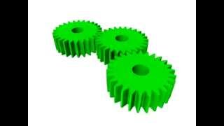
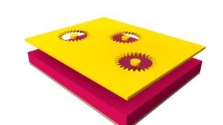
Exactly! By using materials like polysilicon for the structural layer and silicon dioxide for sacrificial layers, we can integrate electronic components easily. What’s a typical application you can think of?

Maybe micro gears and RF MEMS switches?
Yes! Complex microstructures like gears benefit greatly from surface micromachining. Remember that the sacrificial layers must be removed after creating the movable parts; this is key!
High-Aspect-Ratio Micromachining
🔒 Unlock Audio Lesson
Sign up and enroll to listen to this audio lesson
Next, we cover High-Aspect-Ratio Micromachining (HARMS). Why do you think we would create structures with high aspect ratios?
For applications that need tall and narrow geometries, like in biomedical implants.
Exactly! Techniques like the LIGA process and DRIE are fundamental here. Can anyone explain what the LIGA process involves?
It combines deep X-ray lithography with electroplating, right?
Correct! It produces very fine and high structures, which are crucial for specialized devices like microturbines or microfluidic channels. Remember this technique for its critical applications!
Wafer Bonding
🔒 Unlock Audio Lesson
Sign up and enroll to listen to this audio lesson
Let’s dive into wafer bonding. This technique is vital for creating multi-layered MEMS devices. What methods can you recall from our readings?
There’s anodic bonding, which bonds silicon to glass with heat and an electric field.
Good! And what about fusion bonding?
That one reconnects silicon to silicon at a very high surface flatness!
Yes! Remember, wafer bonding methods ensure we can build complex structures and seal spaces like fluidic channels safely. This integration is crucial, especially in pressure sensors and microfluidic systems.
Soft Lithography
🔒 Unlock Audio Lesson
Sign up and enroll to listen to this audio lesson
Lastly, we’ll explore soft lithography techniques which use polymers for fabricating flexible MEMS. What processes can you remember?
I think there’s replica molding where you cast PDMS onto a mold?
Exactly! And why do you think PDMS is commonly used?
It’s flexible and bio-compatible, perfect for medical applications!
Correct! Soft lithography is instrumental for devices like lab-on-chip systems and wearable sensors. Keep in mind the benefits of flexibility and lower costs in MEMS fabrication when using this technique.
Introduction & Overview
Read summaries of the section's main ideas at different levels of detail.
Quick Overview
Standard
The section elaborates on key techniques in MEMS fabrication, detailing processes and applications such as bulk micromachining and surface micromachining. Each method's characteristics, materials used, advantages, and typical applications are presented, underlining their importance and differences.
Detailed
Techniques in MEMS Fabrication
This section provides an overview of essential Techniques in MEMS (Micro-Electro-Mechanical Systems) fabrication. It details the key fabrication methods used to create various microstructures, emphasizing their processes, materials, applications, and strengths.
Key Techniques:
- Bulk Micromachining: Involves the selective etching of silicon wafers to sculpt desired mechanical or electrical components. Common etching techniques include:
- Wet Etching: Utilizes chemical solutions to etch silicon along specific crystal orientations, resulting in angled sidewalls.
-
Dry Etching: Employs plasma-based methods, such as Reactive Ion Etching (RIE) and Deep Reactive Ion Etching (DRIE), to achieve precise vertical walls.
Applications: Pressure sensors, accelerometers, and microsensors. - Surface Micromachining: This method builds microstructures layer by layer on a substrate's surface. Techniques include:
- Deposition of Structural and Sacrificial Layers: These layers allow for the creation of movable parts after the sacrificial layers are etched away.
-
Typical Materials: Polysilicon for structural layers and silicon dioxide for sacrificial layers.
Applications: Micro gears, RF MEMS switches, and micromirrors. - Additional Techniques: Includes techniques like High-Aspect-Ratio Micromachining (HARMS) and Wafer Bonding which cater to specific applications, like microfluidics and biomedical implants.
Each announced method contributes uniquely to the MEMS fabrication landscape, facilitating a diverse range of applications crucial to modern technology.
Youtube Videos
Key Concepts
-
Bulk Micromachining: A selective etching technique that forms structures by removing material from silicon wafers.
-
Surface Micromachining: A method to build microstructures layer by layer on the wafer surface, allowing intricate designs.
-
High-Aspect-Ratio Micromachining (HARMS): Techniques for creating tall and narrow structures, essential for certain applications.
-
Wafer Bonding: Important for sealing and integrating multiple MEMS layers to form complex devices.
Examples & Applications
Applications of bulk micromachining can be seen in pressure sensors that rely on precise etching to create diaphragms.
Surface micromachining is used in RF MEMS switches that require precise layering for performance.
HARMS is notably used in microfluidic devices that require high aspect ratios for functionality.
Memory Aids
Interactive tools to help you remember key concepts
Rhymes
Etching deep, shapes run steep, in silicon's heart, complex parts.
Stories
Imagine a tiny world where layers of silicon grow, each layer adds more, like a cake, to create beautiful microstructures that perform incredible tasks.
Memory Tools
B - Bulk Micromachining, S - Surface Micromachining, H - High-Aspect-Ratio, W - Wafer Bonding, S - Soft Lithography.
Acronyms
MESH - Micromachining Enables Sophisticated Hardware to remember the techniques
Micromachining and Wafer Bonding.
Flash Cards
Glossary
- Bulk Micromachining
A technique that involves the selective removal of material from a silicon wafer to create structures.
- Surface Micromachining
A method that builds microstructures layer by layer on a substrate's surface.
- Wet Etching
A chemical process that dissolves silicon along specific crystal planes using solutions like KOH.
- Dry Etching
A plasma-based technique used for etching that provides better precision and control.
- HARMS
High-Aspect-Ratio Micromachining, used to create tall and narrow microstructures.
- Wafer Bonding
A process used to join multiple substrates or layers in MEMS fabrication.
- Polysilicon
A material commonly used as a structural layer in surface micromachining.
- PDMS
Polydimethylsiloxane, a silicone polymer used in soft lithography.
Reference links
Supplementary resources to enhance your learning experience.