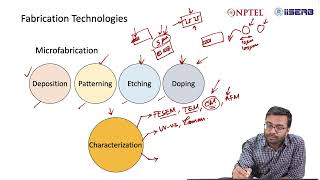
Characterize Semiconductor Materials and Devices
Interactive Audio Lesson
Listen to a student-teacher conversation explaining the topic in a relatable way.
Introduction to Characterization
🔒 Unlock Audio Lesson
Sign up and enroll to listen to this audio lesson

Today, we're starting with characterization, which is the systematic measurement of semiconductor properties. Can anyone tell me why we need to characterize these materials?

To check if they perform as expected?

Exactly! We need to verify material properties, validate fabrication processes, and identify defects or failures. A good acronym for this is V.I.D.: Verify, Identify, and Validate.

What kind of properties do we measure?

Great question! We look at electrical, optical, and structural properties. Each serves a different purpose in understanding the material.
Electrical Characterization Techniques
🔒 Unlock Audio Lesson
Sign up and enroll to listen to this audio lesson

Now, let’s dive into electrical characterization. Who knows about the Four-Point Probe Method?

Isn't that the one that helps eliminate contact resistance errors?

Correct! This method helps us calculate resistivity using the formula ρ = (V/I) × (πt/ln2) for thin films. Can anyone explain why eliminating contact resistance is critical?

Because it can skew our measurements if not corrected?

Exactly! Accurate measurements are vital for understanding the material’s conduction properties. Now let's consider the Hall Effect Measurement. What do we determine using this technique?

Carrier concentration and mobility, right?

Right again! Remember the Hall coefficient: R_H = V_H t / (I×B) is key for this measurement.
Optical Characterization
🔒 Unlock Audio Lesson
Sign up and enroll to listen to this audio lesson

Switching gears, let’s talk about optical characterization. Who can explain the purpose of spectroscopic ellipsometry?

It measures film thickness and the refractive index?

Yes, exactly! It provides insights into the material's optical properties, often fitted with models like Cauchy and Lorentz. Can anyone describe photoluminescence?

It’s used for bandgap determination and identifying defects, right?

Absolutely! Photoluminescence is a powerful tool for analyzing optoelectronic materials.
Introduction & Overview
Read summaries of the section's main ideas at different levels of detail.
Quick Overview
Standard
The section details various techniques used for characterizing semiconductor materials, including electrical (resistivity, Hall effect), optical (spectroscopic ellipsometry, photoluminescence), and structural methods (X-ray diffraction, scanning electron microscopy). It emphasizes the significance of comprehensive characterization in validating materials and fabrication processes.
Detailed
Detailed Summary
This section provides an in-depth exploration of the techniques used to characterize semiconductor materials and devices, crucial for determining their performance and quality.
3.1 Introduction to Characterization
Characterization involves systematic measurement of electrical, optical, and structural properties to validate material properties, fabrication processes, and identify defects.
3.2 Electrical Characterization Techniques
Various electrical techniques such as the Four-Point Probe Method and Hall Effect Measurement are employed to measure resistivity, conductivity, and carrier properties. Additionally, Current-Voltage (I-V) analysis helps in understanding diode behavior and MOSFET performance parameters. The Capacitance-Voltage profiling of MOS capacitors provides insights into doping concentrations and oxide characteristics.
3.3 Optical Characterization
Techniques such as Spectroscopic Ellipsometry and Photoluminescence are used for determining film thickness, bandgap, and defect states, aiding in the understanding of material performance.
3.4 Structural Characterization
Structural methods like X-Ray Diffraction (XRD) and Scanning Electron Microscopy (SEM) reveal essential information about the crystal structure and surface morphology of semiconductor materials.
3.5 Thermal Characterization
Thermal properties are analyzed using techniques such as the 3ω method and laser flash analysis to explore thermal conductivity and thermoelectric properties.
3.6 Device Performance Metrics
Key performance metrics are outlined, including transistor parameters (subthreshold swing, I_on/I_off ratio) and solar cell metrics (open-circuit voltage, short-circuit current).
3.7 Failure Analysis
This section also discusses methods for identifying defects and reliability testing, which are crucial for ensuring the longevity and performance of semiconductor devices.
3.8 Case Study
A case study detailing the characterization of silicon wafers using various techniques makes the section more practical.
3.9 Summary
In conclusion, a comprehensive understanding of semiconductor materials requires leveraging multiple characterization techniques, with electrical measurements being predominant.
Youtube Videos


Audio Book
Dive deep into the subject with an immersive audiobook experience.
Introduction to Characterization
Chapter 1 of 6
🔒 Unlock Audio Chapter
Sign up and enroll to access the full audio experience
Chapter Content
3.1 Introduction to Characterization
- Definition:
- The systematic measurement of electrical, optical, and structural properties of semiconductors to evaluate performance and quality.
- Purpose:
- Verify material properties
- Validate fabrication processes
- Identify defects and failure modes
Detailed Explanation
Characterization of semiconductor materials involves a systematic approach to measuring various properties such as electrical, optical, and structural aspects. This is done to assess how well a semiconductor performs and how high its quality is. The main purposes of characterization are to verify the properties of the semiconductor materials, to check if the fabrication processes have worked correctly, and to identify any defects or potential failure modes in the materials.
Examples & Analogies
Think of characterization like taking a car for a thorough inspection before buying it. Just as an inspector checks the engine, the tires, and the brakes to ensure everything is working correctly, characterization examines semiconductor materials in detail to ensure they will function as intended in electronic devices.
Electrical Characterization Techniques
Chapter 2 of 6
🔒 Unlock Audio Chapter
Sign up and enroll to access the full audio experience
Chapter Content
3.2 Electrical Characterization Techniques
3.2.1 Resistivity and Conductivity
- Four-Point Probe Method:
- Eliminates contact resistance errors
- Resistivity formula: ρ = (V/I) × (πt/ln2) for thin films
- Hall Effect Measurement:
- Determines carrier concentration (n) and mobility (μ)
- Key equations:
- Hall coefficient: R_H = V_H t / (I×B)
- Carrier density: n = 1/(eR_H)
Detailed Explanation
Electrical characterization techniques are crucial for understanding how semiconductors conduct electricity. The Four-Point Probe Method allows us to measure resistivity accurately by eliminating errors that can occur at the points where the probes make contact with the material. The resistivity can be calculated using a specific formula for thin films. The Hall Effect Measurement helps determine important properties of the semiconductor, such as the concentration of charge carriers and their mobility, which can be calculated using the Hall coefficient and other related equations.
Examples & Analogies
Imagine measuring the speed of cars on a highway. Just as you would use sensors spaced apart to ensure accurate speed measurements (avoiding erroneous data from where the cars make contact with the sensor), the Four-Point Probe avoids errors at contact points to get the true resistivity of the material.
Current-Voltage (I-V) Analysis
Chapter 3 of 6
🔒 Unlock Audio Chapter
Sign up and enroll to access the full audio experience
Chapter Content
3.2.2 Current-Voltage (I-V) Analysis
- Diode Characterization:
- Ideal diode equation: I = I_0(e^(qV/nkT) - 1)
- Parameters extracted:
- Saturation current (I_0)
- Ideality factor (n)
- MOSFET Parameters:
- Threshold voltage (V_th)
- Transconductance (g_m = ∂I_D/∂V_GS)
Detailed Explanation
Current-Voltage (I-V) analysis is essential for characterizing diodes and MOSFETs, two crucial components in semiconductor devices. For diodes, the ideal diode equation relates the current flowing through the diode to the voltage across it, allowing for the extraction of important parameters like saturation current and the ideality factor. For MOSFETs, I-V analysis provides key metrics such as the threshold voltage and transconductance, both critical for understanding how effectively the device can control current.
Examples & Analogies
Consider how a faucet controls the flow of water. The I-V analysis is like understanding how much water flows out for a given turn of the faucet (voltage) and helps determine how well the faucet (or MOSFET) can regulate water flow (current).
Capacitance-Voltage (C-V) Profiling
Chapter 4 of 6
🔒 Unlock Audio Chapter
Sign up and enroll to access the full audio experience
Chapter Content
3.2.3 Capacitance-Voltage (C-V) Profiling
- MOS Capacitor Analysis:
- Measures doping concentration (N_A)
- Oxide thickness (t_ox)
- Interface trap density (D_it)
- Key Measurements:
- High-frequency C-V (1MHz)
- Quasi-static C-V
Detailed Explanation
Capacitance-Voltage (C-V) profiling is a technique used to analyze MOS capacitors. It involves measuring capacitance at various voltages, which reveals details about the semiconductor such as doping concentration, oxide thickness, and the density of traps at the interface. Measurements can be taken in two different modes: high-frequency and quasi-static, each providing different insights.
Examples & Analogies
Think of C-V profiling like tuning a musical instrument. Just as adjusting the tension on a string can reveal how well-tuned an instrument is (similar to how different voltage levels reveal material properties), C-V profiling helps us understand the quality and characteristics of semiconductor materials.
Optical Characterization
Chapter 5 of 6
🔒 Unlock Audio Chapter
Sign up and enroll to access the full audio experience
Chapter Content
3.3 Optical Characterization
3.3.1 Spectroscopic Ellipsometry
- Measures:
- Film thickness (sub-nm accuracy)
- Refractive index (n)
- Extinction coefficient (k)
- Data analysis:
- Fitting to optical models (Cauchy, Lorentz)
Detailed Explanation
Optical characterization involves techniques like spectroscopic ellipsometry, which allows scientists to measure film thickness with high precision and determine other important optical properties such as the refractive index and the extinction coefficient of the material. The results are analyzed by fitting the data to established optical models.
Examples & Analogies
Imagine using special glasses that can measure how thick a piece of glass is while also telling you how light bends when it passes through. Just like these glasses would help you understand the properties of light passing through glass, spectroscopic ellipsometry helps evaluate the optical properties of semiconductor films.
Summary
Chapter 6 of 6
🔒 Unlock Audio Chapter
Sign up and enroll to access the full audio experience
Chapter Content
3.9 Summary
- Comprehensive characterization requires multiple techniques
- Electrical measurements dominate device evaluation
- Structural and optical methods complement electrical data
- Standardized protocols ensure reproducible results
Detailed Explanation
In summary, effectively characterizing semiconductor materials and devices mandates using various techniques. While electrical measurements are the most critical for evaluating devices, structural and optical methods provide vital complementary information. Moreover, following standardized protocols is crucial for ensuring that the results are consistent and replicable across different studies.
Examples & Analogies
Think of characterizing semiconductor materials as conducting a thorough health check-up for a person. Just as doctors use various tests (blood pressure, blood tests, X-rays) to assess overall health, using various characterization techniques gives a holistic view of a semiconductor's quality and performance.
Key Concepts
-
Characterization: The process of measuring material properties to understand performance and quality.
-
Electrical Techniques: Methods like Four-point probe and Hall effect to assess resistivity and conductivity.
-
Optical Techniques: Spectroscopic ellipsometry and photoluminescence used for analyzing film properties.
-
Structural Techniques: X-ray diffraction and scanning electron microscopy that provide insights into the material structure.
-
Thermal Characterization: Understanding materials’ thermal properties, crucial for performance evaluation.
Examples & Applications
A Four-Point Probe setup yielding a resistivity of a silicon film.
Using X-Ray Diffraction to identify the (111) peak of a silicon wafer.
Memory Aids
Interactive tools to help you remember key concepts
Rhymes
To measure PEACE, you need to sense the conductivity and resistance hence.
Stories
Imagine a bustling city where the flow of traffic mirrors the flow of electrons, with traffic lights that represent resistivity guiding the flow.
Memory Tools
Remember the acronym C.O.S.T. for key characterization techniques: Characterization, Optical, Structural, Thermal.
Acronyms
Use the acronym 'E.O.S.' to remember Electronic, Optical, and Structural properties when characterizing.
Flash Cards
Glossary
- Resistivity
A measure of how strongly a material opposes the flow of electric current.
- Hall Effect
The production of voltage across a conductor when it is placed in a magnetic field.
- Spectroscopic Ellipsometry
An optical technique used to measure film thickness and refractive indices.
- Photoluminescence
The emission of light from material after it absorbs photons.
- Xray Diffraction (XRD)
A tool used to study the crystal structure of materials.
Reference links
Supplementary resources to enhance your learning experience.
