
Current Mirror Load
Interactive Audio Lesson
Listen to a student-teacher conversation explaining the topic in a relatable way.
Introduction to Current Mirroring
🔒 Unlock Audio Lesson
Sign up and enroll to listen to this audio lesson

Today, we're going to explore Current Mirror Loads in MOSFET amplifiers. Can anyone tell me what a current mirror does, and why it might be preferred over a simple resistor load?

A current mirror replicates the current flowing through one active device to another, right?
Exactly! And by doing this, we can achieve high DC gain without the area penalty associated with passive components like resistors. What do you think would be the main advantages of this approach?

We have higher gain, and it saves space on the chip!
That's correct! Let's remember this with the acronym GAIN: Gain, Active load, Integrated circuit design, and No resistor!

I like that! It’s easy to remember.
Great! Now, what are the specific advantages we get with a current mirror configuration?

High DC gain, improved matching, and better thermal stability!
Well done! Let's summarize: Current mirrors are efficient for high DC gain and use fewer physical resources.
Key Equations and Gain Enhancement
🔒 Unlock Audio Lesson
Sign up and enroll to listen to this audio lesson

Now that we've understood the basics, let's discuss how to calculate the gain. The gain can be calculated as follows: A_V ≈ -g_m(r_o1 || r_o2). Can someone explain what g_m stands for?
g_m is the transconductance, it measures how effectively input voltage controls the output current!
Exactly! And when we consider multiple stages, say a cascode, what do you think might happen to the gain?
It would probably increase a lot due to the multiplication effect!
Correct! The enhancement can be expressed as A_V ≈ -g_{m1}(g_{m2}r_{o2}r_{o1}), which can increase the gain by a factor of 10 to 100 times. What do you think this means for amplifier design?
We can achieve higher performance with fewer components!
Rightly said! This efficiency is critical in modern circuit design. Let’s remember this enhancement with the phrase: 'Higher gain gets great features!'
Application of Current Mirror in Circuit Design
🔒 Unlock Audio Lesson
Sign up and enroll to listen to this audio lesson
With our understanding of current mirrors, let's discuss their applications. Why do you think current mirrors are vital in amplifiers?
They allow us to make compact designs while maximizing performance!
That's right! Also, what about thermal stability—how does this circuit help with that?
They maintain current more precisely, reducing variations with temperature!
Exactly! More stable currents mean better performance over varying temperatures. And to wrap up today, can anyone recall why minimizing the use of resistors is beneficial?
Because it saves area and reduces power consumption!
Fantastic! Always remember that in modern design, efficiency is king!
Introduction & Overview
Read summaries of the section's main ideas at different levels of detail.
Quick Overview
Standard
Current Mirror Load configurations enhance the performance of MOSFET amplifiers by providing high DC gain. This section explains the structure of the current mirror load, its advantages over traditional resistive loads, and introduces the concept of using cascaded stages to further increase gain.
Detailed
Current Mirror Load - Detailed Summary
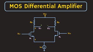
Current mirror loads are essential in improving the gain of MOSFET amplifier circuits. By employing a current mirror, which typically consists of matched transistor pairs, one can achieve high DC gain without using resistors that occupy physical area and decrease performance. The fundamental structure includes a PMOS transistor (Q2) and an NMOS transistor (Q1), providing the basic configuration for the current mirror in a differential amplifier.
The gain of the current mirror load can be expressed approximately as:
\[ A_V \approx -g_{m1}(r_{o1} \parallel r_{o2}) \]
Where \( g_{m1} \) is the transconductance of the NMOS transistor and \( r_{o1} \) and \( r_{o2} \) are the output resistances of the respective devices.
Additionally, to enhance the gain further, a cascode stage may be introduced, leading to substantial increases in gain by factors ranging from 10 to 100 times:
\[ A_V \approx -g_{m1}(g_{m2}r_{o2}r_{o1}) \]
This approach not only conserves area but significantly improves performance metrics like output impedance and linear range.
Youtube Videos

Audio Book
Dive deep into the subject with an immersive audiobook experience.
Current Mirror Load Configuration
Chapter 1 of 2
🔒 Unlock Audio Chapter
Sign up and enroll to access the full audio experience
Chapter Content
VDD
│
Q2 (PMOS)
│
D───Vout
G───┤
│
Q1 (NMOS)
│
GND
Detailed Explanation
This chunk describes the configuration of a current mirror load using two transistors: a PMOS transistor (Q2) and an NMOS transistor (Q1). In this arrangement, the PMOS transistor is connected to a positive supply voltage (VDD) and the NMOS transistor connects to ground. The important points in this configuration are how the output voltage (Vout) is taken from the drain of the PMOS transistor. This setup allows for precise copying of current, which is crucial in analog circuits.
Examples & Analogies
Think of the current mirror like a copier in an office. The PMOS transistor is the copier that gets powered (VDD) while the NMOS transistor can be seen as the receiving end that accepts the copied documents (current). Just as you make identical copies of documents, the current mirror ensures that the current flowing through Q2 mirrors the current that flows through Q1.
Advantages of Current Mirror Load
Chapter 2 of 2
🔒 Unlock Audio Chapter
Sign up and enroll to access the full audio experience
Chapter Content
- Advantages:
- High DC gain (AV ≈ -gm1(ro1ǁro2))
- No resistor area penalty
Detailed Explanation
The use of a current mirror load presents several advantages. First, it provides high DC gain, which is indicated by the formula where AV is approximately equal to the negative product of the transconductance (gm1) of the first transistor and the parallel resistance of the output resistances (ro1 and ro2) of both transistors. This means that the current mirror can significantly amplify the signal without needing additional components that would otherwise take up space on a circuit board.
Examples & Analogies
Imagine a bakery where you use a specific recipe (the design of the current mirror) to create a large batch of cookies (high gain). You’re able to produce many cookies without using extra baking trays (no resistor area penalty). This allows you to efficiently use your available baking space while maximizing your output.
Key Concepts
-
Current Mirror: A circuit configuration that replicates an input current into another output.
-
g_m (Transconductance): Measures the efficiency of controlling output current via input voltage.
-
r_o (Output Resistance): Important for calculating amplifier gain.
-
Cascode: A method to enhance gain by using stacked transistors.
Examples & Applications
Implementing a Current Mirror Load in a Common-Source Amplifier to achieve 20x gain.
Using a cascode stage with a current mirror to boost overall DC gain.
Memory Aids
Interactive tools to help you remember key concepts
Rhymes
In the circuits where currents align, mirrors reflect without decline.
Stories
Imagine a busy manager who uses mirrors to reflect the workload onto other assistants; this is how a current mirror ensures that the output mirrors the input, effectively managing the current flow.
Memory Tools
Remember 'MIRRORS': Magnitude, Input, Replicate, Resistor-free, Output, Reliability, Stability.
Acronyms
G.A.I.N. - Gain, Active load, Integrated circuit design, No resistors!
Flash Cards
Glossary
- Current Mirror
A circuit that copies the current flowing in one active device to another, providing stable biasing and increased gain.
- Transconductance (g_m)
A measure of how well a transistor can convert a change in input voltage into a change in output current.
- Output Resistance (r_o)
The resistance seen by the output of a current source, contributing to voltage gain in amplifiers.
- Cascode Stage
A voltage amplifier stage that increases the output impedance and enhances gain by stacking transistors.
Reference links
Supplementary resources to enhance your learning experience.