
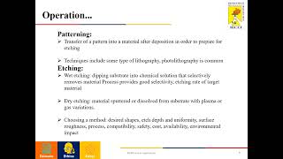
Fabrication Techniques
Enroll to start learning
You’ve not yet enrolled in this course. Please enroll for free to listen to audio lessons, classroom podcasts and take practice test.
Interactive Audio Lesson
Listen to a student-teacher conversation explaining the topic in a relatable way.
Bulk Micromachining
🔒 Unlock Audio Lesson
Sign up and enroll to listen to this audio lesson

Today, we will start with bulk micromachining. This technique allows us to create mechanical structures by removing material from a silicon substrate. Why do you think this is important in MEMS?

It's important because it helps shape the devices we build!
Exactly! Bulk micromachining enables complex 3D shapes. Remember, think of the acronym 'TRIM' - for *T*hree-dimensional, *R*emove, *I*ntegration of, and *M*icrostructures. Can anyone give me an example of a device that uses this technique?

Maybe accelerometers!
That's right, accelerometers often use bulk micromachining to sense movements!
Surface Micromachining
🔒 Unlock Audio Lesson
Sign up and enroll to listen to this audio lesson

Now, let's transition to surface micromachining. This method involves building structures on the surface of a substrate layer by layer. Why might this method be advantageous?

It allows for more versatility in design with different materials!
Great point! This layering technique supports various functionalities. Let's remember 'LAYER' - *L*ayered, *A*pplications, *Y*ield, *E*nhanced, *R*esults. Can anyone share a practical example of devices made via surface micromachining?

I think MEMS microphones would be one example?
Spot on! MEMS microphones often utilize surface micromachining due to their complex layered structure.
LIGA Process
🔒 Unlock Audio Lesson
Sign up and enroll to listen to this audio lesson
Next up is LIGA, which stands for Lithographie, Galvanoformung, Abformung. Have any of you heard about its usage?
I think it’s used for making very precise components, right?
Absolutely! LIGA allows for high-aspect-ratio structures that are very precise. Remember the mnemonic ‘LIG(tA)’ for *L*ithography, *I*ntegration, *G*alvanic, and *A*bformung. What kind of applications do you think benefit from this precision?
Probably optics and sensors?
Correct! It’s widely used in optical devices and other areas requiring detailed microfabrication.
Wafer Bonding
🔒 Unlock Audio Lesson
Sign up and enroll to listen to this audio lesson
Lastly, let’s talk about wafer bonding. It’s crucial for packaging MEMS devices effectively. How does wafer bonding enhance our MEMS?
It keeps all layers sealed and safe!
Exactly! Wafer bonding maintains the integrity and functionality of MEMS devices. Can anyone recall the key steps involved in wafer bonding?
Preparing, aligning, and heating the wafers?
Perfect! Let’s summarize: wafer bonding is key to ensuring the longevity and performance of MEMS. The acronym 'SURE' can help you remember: *S*eal, *U*nify, *R*eason, *E*ffectively.
Introduction & Overview
Read summaries of the section's main ideas at different levels of detail.
Quick Overview
Standard
The section details key fabrication techniques in microelectromechanical systems (MEMS), explaining the processes of bulk micromachining, surface micromachining, LIGA, and wafer bonding, and how they contribute to creating precise mechanical structures and devices on silicon substrates.
Detailed
In MEMS fabrication, several techniques are integral in producing miniature devices that combine both mechanical and electronic components. This section discusses four primary methods:
- Bulk Micromachining: This technique involves the removal of material (usually silicon) from a substrate, allowing the creation of mechanical structures beneath the surface. It is crucial for forming intricate 3D structures necessary for MEMS functionality.
- Surface Micromachining: Unlike bulk micromachining, surface micromachining builds structure layer by layer on the surface of the substrate. This technique allows for the integration of multiple layers of different materials, enabling more complex MEMS designs with diverse functionalities.
- LIGA (Lithographie, Galvanoformung, Abformung): A specialized fabrication method that uses deep X-ray lithography to create high-aspect-ratio microstructures. LIGA is ideal for applications requiring precise and deep structures, such as optical and mechanical components.
- Wafer Bonding: This technique is essential for stacking and sealing MEMS layers to ensure protection and packaging of the devices made. It involves bonding two or more wafers together, enhancing device functionality and durability.
Understanding these fabrication techniques is critical for engineers and designers in the MEMS field, as they influence the performance, reliability, and capabilities of the devices developed.
Youtube Videos


Audio Book
Dive deep into the subject with an immersive audiobook experience.
Overview of MEMS Fabrication Techniques
Chapter 1 of 5
🔒 Unlock Audio Chapter
Sign up and enroll to access the full audio experience
Chapter Content
MEMS fabrication leverages traditional semiconductor processes along with specialized micromachining techniques:
Detailed Explanation
MEMS fabrication is a crucial process in creating microelectromechanical systems. This process combines traditional methods used in semiconductor manufacturing with specialized techniques designed for microscale applications. Essentially, it allows for the creation of tiny structures and components that are fundamental to MEMS devices. By utilizing established semiconductor techniques, manufacturers can ensure precision and efficiency in producing these advanced microsystems.
Examples & Analogies
Think of MEMS fabrication like assembling a jigsaw puzzle, where traditional semiconductor processes represent the image guide to how the pieces fit together while specialized micromachining techniques are like the unique shapes that help you form a specific picture with those pieces.
Bulk Micromachining
Chapter 2 of 5
🔒 Unlock Audio Chapter
Sign up and enroll to access the full audio experience
Chapter Content
● Bulk Micromachining: Removes material from the silicon substrate to create mechanical structures.
Detailed Explanation
Bulk micromachining is a technique used in MEMS fabrication where material is selectively removed from a silicon substrate. This process allows manufacturers to carve out three-dimensional structures necessary for creating mechanical components such as beams and sensors. Essentially, by 'excavating' parts of the silicon, they can form intricate shapes and designs that make up the functional elements of a MEMS device.
Examples & Analogies
Imagine bulk micromachining as sculpting a statue from a block of marble. Just as a sculptor chisels away excess stone to reveal a beautiful statue, engineers remove silicon in specific areas to design complex mechanical structures.
Surface Micromachining
Chapter 3 of 5
🔒 Unlock Audio Chapter
Sign up and enroll to access the full audio experience
Chapter Content
● Surface Micromachining: Builds microstructures layer by layer on the substrate surface.
Detailed Explanation
Surface micromachining is a method where thin films of material are deposited onto the surface of a silicon substrate. Unlike bulk micromachining, this technique constructs structures layer by layer, allowing for greater detail and complexity in the final product. This process is critical for creating delicate mechanical elements that can move or flex, such as springs or actuators. By adding materials one layer at a time, engineers can carefully control the shape and thickness of the microstructures.
Examples & Analogies
Think of surface micromachining like building a cake with layers. Each layer of cake represents a microstructure added to the substrate. Just as the cake grows taller and takes shape with each added layer, MEMS devices build intricate structures that perform specific functions, layer by layer.
LIGA Technique
Chapter 4 of 5
🔒 Unlock Audio Chapter
Sign up and enroll to access the full audio experience
Chapter Content
● LIGA (Lithographie, Galvanoformung, Abformung): A high-aspect-ratio fabrication technique that uses deep X-ray lithography.
Detailed Explanation
The LIGA technique combines lithography, electroforming, and molding to create high-aspect-ratio microstructures. This technique is particularly exceptional in producing tall and thin structures, which are essential in MEMS applications that require a high level of precision and verticality. By using deep X-ray lithography, engineers can expose thick photoresist to create molds that can be filled with metal or polymers to achieve the final desired shapes.
Examples & Analogies
Consider the LIGA technique akin to creating ice sculptures using a mold. The initial mold represents the lithography process, and pouring water into the mold to freeze is similar to the electroforming process. The final sculpture comes out detailed and precisely shaped, just like the microstructures developed through LIGA.
Wafer Bonding
Chapter 5 of 5
🔒 Unlock Audio Chapter
Sign up and enroll to access the full audio experience
Chapter Content
● Wafer Bonding: Used to stack and seal MEMS layers to protect and package them effectively.
Detailed Explanation
Wafer bonding is a process that involves joining multiple silicon wafers together to form a more complex structure, offering protection and sealing for the MEMS devices. This technique is crucial as it enables the integration of different layers that can contain various functionalities, ensuring that the final MEMS device is robust and efficient. Adequate sealing also protects the delicate microstructures from environmental factors that could affect their performance.
Examples & Analogies
Think of wafer bonding like layering a cake with icing between each layer for preservation and flavor. Just as icing seals layers together and protects them, wafer bonding securely fuses different silicon layers, enhancing the overall functionality and reliability of MEMS devices.
Key Concepts
-
Bulk Micromachining: Technique for creating three-dimensional structures by removing substrate material.
-
Surface Micromachining: Builds complex structures through a layer-by-layer process.
-
LIGA: A precise method for creating high-aspect-ratio microstructures using deep X-ray lithography.
-
Wafer Bonding: A process that seals and stacks MEMS layers, enhancing protection and functionality.
Examples & Applications
MEMS accelerometers use bulk micromachining to sense motion and acceleration changes.
MEMS microphones utilize surface micromachining for their intricate layered designs.
Memory Aids
Interactive tools to help you remember key concepts
Rhymes
In MEMS fabrication, ‘micromachine,’ / Bulk or layer, are part of the scene.
Stories
Imagine a sculptor chipping away at a stone to create a statue (bulk micromachining). Then visualize a cake being constructed layer by layer, each topping a new addition (surface micromachining). Lastly, imagine stacking boxes securely to keep contents safe (wafer bonding).
Memory Tools
For LIGA, think Lithographic, Interface, Galvanoformung, Abformung. Remember 'LIG(tA)'!
Acronyms
Use 'BULK' to remember
*B*uilding
*U*nderstand
*L*ayers
*K*eeping structures.
Flash Cards
Glossary
- Bulk Micromachining
A fabrication technique that removes material from a silicon substrate to create three-dimensional mechanical structures.
- Surface Micromachining
A technique that builds structures layer by layer on the surface of a substrate material.
- LIGA
A fabrication method that uses lithography, electroplating, and polymer molding for constructing high-aspect-ratio microstructures.
- Wafer Bonding
The process of stacking and sealing MEMS layers together to protect and package them.
Reference links
Supplementary resources to enhance your learning experience.