
Additional Components Consideration
Enroll to start learning
You’ve not yet enrolled in this course. Please enroll for free to listen to audio lessons, classroom podcasts and take practice test.
Interactive Audio Lesson
Listen to a student-teacher conversation explaining the topic in a relatable way.
Voltage Gain Analysis in Common Collector Amplifiers
🔒 Unlock Audio Lesson
Sign up and enroll to listen to this audio lesson

Let's begin with the common collector amplifier. Can anyone tell me the significance of the collector resistance in determining voltage gain?

I think it affects the overall voltage gain by creating a load on the collector.
Exactly, while it does introduce some resistance, the voltage gain remains approximately one. This is crucial because it means that the amplifier works as a buffer. Remember this with the acronym V.G. - Voltage Gain is close to 1.

But how can we mathematically show that?
Great question! We can derive that by analyzing the relationship between the input voltage and the output voltage through Kirchhoff’s laws and current relationships, leading us to derive expressions impacting the gain.

So if the gain is almost 1, is there no effect from external components?
Not quite! While the voltage gain approximates 1, external components like resistances do affect input and output impedances. Let's transition into input resistance next.

How does the input resistance factor in?
Fantastic! The input resistance increases due to parallel connections with components like resistors, crucial for understanding how the amplifier interacts with subsequent stages in a circuit.
Input and Output Resistance Analysis
🔒 Unlock Audio Lesson
Sign up and enroll to listen to this audio lesson

Continuing from our last discussion, let’s analyze the input resistance. Who can explain how it is derived?
I remember that it involves finding the current at the input terminal?
Exactly! By applying KCL at the emitter node, you can express it in terms of base currents, leading to a comprehensive understanding of resistance.
What about the output resistance?
Good! For output resistance, we consider the circuit excited with a voltage source while treating the input AC ground. This allows us to derive the output in relationship to the load. The key takeaway is that output resistance is a measure of how well the circuit can drive loads without significant voltage drop.
So, the impacts of resistances are different on input and output sides?
Exactly! While both are critical, their relationships to how the circuit interacts with other stages vary and essentially dictate the amplifier's performance.
Can we apply this to other configurations like the common drain?
Yes! The principles are similar, and we can explore those next.
Common Drain Amplifier Analysis
🔒 Unlock Audio Lesson
Sign up and enroll to listen to this audio lesson
Now, shifting gears to the common drain amplifier. What peculiarities can we expect here compared to the common collector?
I believe it won't have an internal resistance like in BJTs.
That's right! We won't have a similar resistance, but we must still evaluate voltage gain and input capacitance. Let's explore how voltage gain behaves in this setup.
How do we find the voltage gain?
By using similar equations we derived for common collectors, but we can simplify it further since certain parameters like r are quite high, often leading to the gain being approximately equal to 1. Remember: Voltage Gain Common Drain is V.G.C.D. = 1!
What about capacitance?
Excellent question! The input capacitance inherits traits from both Cgs and Cgd with Miller effects as well. We should examine how that translates to our calculations in real circuits.
So, both types have low input capacitance?
Yes! This characteristic is common and beneficial, particularly for buffer-like applications where isolating stages is essential.
Practical Application and Numerical Examples
🔒 Unlock Audio Lesson
Sign up and enroll to listen to this audio lesson
As we reflect on our findings, how can we apply these concepts practically?
We can analyze real circuits using these parameters!
Absolutely! For example, let’s say we have a common collector amplifier with a specific load resistance. What would you do first?
I would calculate the current flowing and use that to find voltage gain.
Exactly, that's a solid approach! It’s crucial to look at factors like load resistance to impact overall performance. What further steps would you take?
I'd also assess input and output resistances to ensure compatibility with other stages.
Spot on! Matching these parameters is vital in circuit design. How might we document our findings?
Maybe by maintaining a design log with calculations and observations.
Excellent! Proper documentation allows us to understand design trade-offs and performance expectations for future modifications.
Introduction & Overview
Read summaries of the section's main ideas at different levels of detail.
Quick Overview
Standard
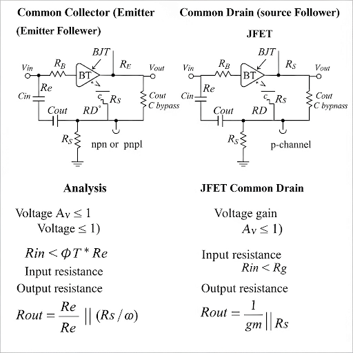
The discussion revolves around the common collector and common drain amplifier configurations, highlighting their voltage gain, input and output resistance, and input capacitance. It provides mathematical derivations and conceptual explanations regarding how additional components affect circuit behavior and performance, with analytical insights into small signal models.
Detailed
In this section, we delve into the behavior and analysis of common collector and common drain amplifiers concerning various components. Beginning with the common collector setup, we analyze the impact of the collector resistance on the voltage gain, emphasizing that the voltage gain remains close to one despite these resistances. Next, we calculate the input and output resistances and examine how the additional collector resistance influences overall input impedance, leading to higher values that favor circuit performance. We shift focus to input capacitance, noting how the Miller effect comes into play with input capacitance being influenced by voltage gain factors leading to practical approximations for circuit designs. Similarly, we analyze the common drain configuration with no significant internal resistance from a MOSFET perspective, ultimately drawing parallels to the common collector analysis. The importance of understanding these parameters is pronounced for effective circuit design and performance evaluation.
Youtube Videos

Audio Book
Dive deep into the subject with an immersive audiobook experience.
Voltage Gain in Common Collector Configuration
Chapter 1 of 4
🔒 Unlock Audio Chapter
Sign up and enroll to access the full audio experience
Chapter Content
The voltage gain is essentially determined from the relationship between the output voltage and the input voltage, v_o = v(in). This shows that the gain is approximately 1.
Detailed Explanation
In a common collector amplifier configuration, the voltage gain can be described by the output voltage (v_o) being nearly equal to the input voltage (v_in). This approximation indicates that the amplifier does not significantly increase the voltage level. Thus, it acts more like a buffer. The relationship implies little amplification, which is typical of common collector stages due to their inherent design.
Examples & Analogies
Think of the common collector amplifier as a water pipeline that delivers water from a large tank. If the tank level remains the same regardless of how much water flows out (just like the output voltage being close to the input voltage), we can say it is maintaining a consistent level rather than amplifying or reducing it. This consistency in water level signifies the characteristic buffer behavior of the amplifier.
Input Resistance
Chapter 2 of 4
🔒 Unlock Audio Chapter
Sign up and enroll to access the full audio experience
Chapter Content
The input resistance can be derived from the base terminal current (i_b) and voltage across it (V), establishing the relationship that if R is high, the overall input resistance is increased significantly.
Detailed Explanation
The input resistance of a common collector amplifier is influenced by the resistance at the input terminals, which is dependent on the base terminal current and the voltage applied. As the resistance R is applied in series with the base terminal, it directly increases the overall input resistance. This higher input resistance is beneficial for preventing loading effects in the circuits connected to the amplifier, thus ensuring better signal integrity.
Examples & Analogies
Imagine a sponge absorbing water. A higher resistance at the input is like a sponge that has large pores and can hold more water without affecting the overall flow of water from a source. Just like the sponge doesn't obstruct the water flow significantly, a high input resistance ensures that the amplifier does not interfere with the signal it is processing.
Output Resistance
Chapter 3 of 4
🔒 Unlock Audio Chapter
Sign up and enroll to access the full audio experience
Chapter Content
To find the output resistance, the analysis involves making the input signal an AC ground and observing the current flow through resistive components.
Detailed Explanation
Output resistance in the common collector configuration is evaluated by considering the outputs when the input is grounded, allowing us to measure how much resistance is present at the output terminal when stimulated by a voltage source. This method leads to a calculated output resistance that tends to be low when typically examined with resistors in parallel, making it suitable for driving loads without significant voltage drop.
Examples & Analogies
Think of output resistance as a water hose. If the hose is wide (low output resistance), water flows freely with less pressure drop, which is ideal for driving a garden sprinkler (the load). Conversely, a narrow hose (high output resistance) would restrict water flow and decrease performance, so the goal is to have an adequately wide hose to maintain good water flow.
Input Capacitance
Chapter 4 of 4
🔒 Unlock Audio Chapter
Sign up and enroll to access the full audio experience
Chapter Content
The input capacitance at the base terminal incorporates the effects of two capacitors, where their contributions are affected by the voltage gain.
Detailed Explanation
Input capacitance in a common collector amplifier is influenced by the capacitors connected at the input nodes. The effective capacitance is calculated by considering how the voltage gain influences the voltage across the capacitors, which leads to the conclusion that the overall capacitance impacts the frequency response of the amplifier. Higher input capacitance can lead to reduced performance at higher frequencies, thus the design must account for this.
Examples & Analogies
Consider input capacitance as a large bucket that collects rainwater. The faster it fills up (lower capacitance), the quicker it can be emptied. However, if the bucket is large (high capacitance), it takes longer to fill, which might delay the response in terms of how quickly we can use that water. This illustrates why managing input capacitance is crucial for maintaining quick response times in amplifiers.
Key Concepts
-
Common Collector Amplifier: An amplifier configuration that provides voltage buffering with a gain close to one.
-
Input Resistance: The impedance which an external circuit 'sees' at the input of the amplifier.
-
Output Resistance: An important parameter that affects the ability of an amplifier to drive loads efficiently.
-
Miller Effect: A phenomenon where the input and output capacitances affect the overall input capacitance due to amplification.
Examples & Applications
Example 1: A common collector amplifier with a collector resistance of 1kΩ shows a voltage gain of approximately 1, despite load changes due to the resistive value.
Example 2: A common drain amplifier designed with a gate-source capacitance of 10pF and a calculated voltage gain of 0.98 reflects low input capacitance behavior relevant in high-frequency applications.
Memory Aids
Interactive tools to help you remember key concepts
Rhymes
When voltage gain is close to one, output buffering can be lots of fun!
Stories
A circuit engineer designed a buffer with minimal resistance, ensuring signals remained strong and clear. This became the go-to solution for audio applications where quality matters!
Memory Tools
Remember 'I.R. and O.R.' for Input Resistance and Output Resistance with input growing and output flowing.
Acronyms
V.G. - for Voltage Gain, nearly 1 helps engineers maintain optimum circuit dynamics.
Flash Cards
Glossary
- Voltage Gain
The ratio of output voltage to input voltage in an amplifier, indicating amplification.
- Input Resistance
The resistance seen by the input signal in a circuit, critical for determining how an amplifier interacts with previous stages.
- Output Resistance
The resistance presented by the output of an amplifier to the load, impacting the ability to drive subsequent components.
- Input Capacitance
The capacitance presented to the input signal, which can affect frequency response and stability in amplifiers.
Reference links
Supplementary resources to enhance your learning experience.