
Input Capacitance Analysis
Enroll to start learning
You’ve not yet enrolled in this course. Please enroll for free to listen to audio lessons, classroom podcasts and take practice test.
Interactive Audio Lesson
Listen to a student-teacher conversation explaining the topic in a relatable way.
Introduction to Common Collector Amplifiers
🔒 Unlock Audio Lesson
Sign up and enroll to listen to this audio lesson

Today we're diving into common collector amplifiers. Can anyone tell me what they think is unique about a common collector configuration?

I think it has low output resistance?
Excellent! The common collector indeed has low output resistance, making it behave as a voltage buffer. This helps keep the voltage gain close to 1.

What about the input and output characteristics?
Great question! The input resistance is typically high, which is favorable in many applications. Remember, we can use the acronym 'HIV' for High Input Voltage.

Got it! So, high input and low output – that sounds like a good combo!
Exactly! Let's summarize: Common collector amplifiers provide high input impedance and low output impedance, facilitating better performance as a buffer.
Application of Kirchhoff's Current Law
🔒 Unlock Audio Lesson
Sign up and enroll to listen to this audio lesson

Next, we need to understand Kirchhoff's Current Law in the context of our amplifier circuits. What does KCL signify for us?

It states that the sum of currents entering a junction equals the sum of currents leaving the junction?
Exactly! In our CC amplifier, we can balance the base current and the emitter current. Can someone relate this to what we've discussed about the base current?
Since the base current flows toward the ground, it converges with the emitter current.
Yes! That's critical to remember. This connects to our next topic of analyzing the voltage gain equation. Who can describe how we derive it?
Voltage Gain Analysis
🔒 Unlock Audio Lesson
Sign up and enroll to listen to this audio lesson
Let's derive our voltage gain formula. Starting with our relationship between output voltage and input voltage, what connects these two?
It seems to depend on the resistances in the circuit, right?
Correct! The impedance at play helps determine the voltage gain. Can anyone remember the approximate value of the voltage gain in ideal conditions?
It approaches 1!
Exactly! Now, why is that significant, particularly in buffer applications?
It ensures that we can effectively transfer the input signal with minimal distortion.
Great answer! So, buffering helps maintain signal integrity, which is fundamental in circuit design.
Output Resistance in Circuit Design
🔒 Unlock Audio Lesson
Sign up and enroll to listen to this audio lesson
Now let's discuss output resistance. Why is understanding this characteristic critical in our analysis?
It helps us know how the amplifier interacts with different loads.
Exactly! And what can happen if the output resistance is too high?
It can lead to a voltage drop and poor performance with loads.
Right! Therefore, we often want our output resistance to be low with respect to the load. Why do we want this?
To ensure that maximum voltage and power are delivered to the load!
To summarize, understanding output resistance helps us avoid performance issues when interfacing components.
Input Capacitance Considerations
🔒 Unlock Audio Lesson
Sign up and enroll to listen to this audio lesson
Finally, we need to consider input capacitance. Who can explain why this is an important factor?
It affects how fast the circuit can respond to changes in input voltage!
Absolutely! And what factors influence input capacitance in our circuits?
The types of resistances we connect and the capacitive components across the terminal!
Correct! Input capacitance is often a combination of multiple factors. Can anyone summarize what we've learned about its impact?
It’s low in common collector configurations, ensuring high-speed response.
Exactly! So, low input capacitance is beneficial for high-frequency applications. Well done everyone!
Introduction & Overview
Read summaries of the section's main ideas at different levels of detail.
Quick Overview
Standard
Focusing on input capacitance, this section elaborates on the small signal equivalent circuit, calculating input resistance and output resistance. The analysis emphasizes how resistances can impact voltage gain and capacitances in common collector and common drain configurations.
Detailed
Detailed Summary
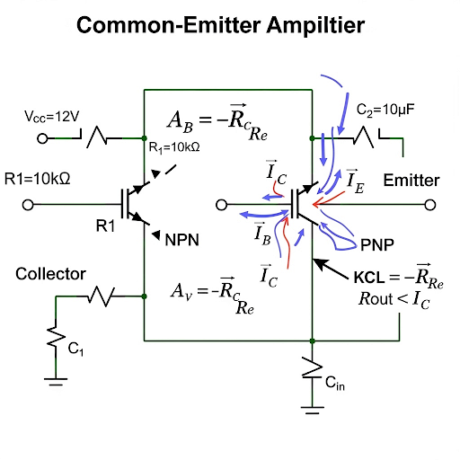
The section on Input Capacitance Analysis provides an essential examination of the role of capacitance in common collector (CC) and common drain (CD) amplifiers. The analysis begins with a review of the small signal equivalent circuit, highlighting the significance of input voltage applied at the base and the effects of collector voltage on the overall circuit operation.
Key Points Covered:
- Understanding Collector and Emitter Dynamics: The collector terminal's voltage is significant as it is not considered AC ground and can influence the base current.
- Kirchhoff's Current Law (KCL): KCL application at the emitter node is critical, as it balances the current through the active device and the base current.
- Voltage Gain and Input Resistance: The output voltage is related to the input voltage through voltage gain, closely approximated by 1 in conditions with high resistance R.
- Output Resistance Analysis: A deeper look into output resistance reveals the need to account for current through the device in both ideal and practical scenarios, ultimately leading to approximations based on component values.
-
Input Capacitance Considerations: The section builds on capacitance analysis, showing how it ties into the overall performance of the amplifier, affected by resistances and connections within the circuit.
By understanding these principles, students gain insights into the designs of circuits involving BJTs and MOSFETs, aiding in the analysis and troubleshooting of real-world applications.
Youtube Videos

Audio Book
Dive deep into the subject with an immersive audiobook experience.
Introduction to Input Capacitance
Chapter 1 of 4
🔒 Unlock Audio Chapter
Sign up and enroll to access the full audio experience
Chapter Content
Yes. So, things are getting really getting complicated, let us see what are the complications are getting here. So, we do have the small signal equivalent circuit, we do have the C and then, C and note that compared to our previous discussion, the voltage here it is not AC ground rather voltage it is v and v , it is of course, it is function of input voltage.
Detailed Explanation
This chunk introduces the concept of input capacitance in the context of the small signal equivalent circuit. It highlights that the analysis is more complex than previous discussions. Here, 'C' refers to capacitances in the circuit that affect the overall behavior when signals are applied. Unlike prior scenarios where voltages might be simply considered as AC ground (a reference point), this situation involves voltages that change based on the input voltage.
Examples & Analogies
Imagine adjusting the volume on a stereo system. Initially, when there is no sound (like AC ground), the system is easy to understand. However, once you start playing different tunes at various volumes, the sound quality changes and requires a more nuanced understanding of how the components (e.g., speakers and amps) interact, similar to how C interacts with voltage in our circuit.
Expressing Output Voltage
Chapter 2 of 4
🔒 Unlock Audio Chapter
Sign up and enroll to access the full audio experience
Chapter Content
Now, we may recall that the voltage at the output node v , we already have this expression of this v in terms of v having this factor. So, numerator it is smaller than the denominator by this r and then, the expression of the of the v , it is the R multiplied by whatever the current is flowing and that is that we have discussed before.
Detailed Explanation
This chunk describes how the output voltage is derived from the input voltage expression. It notes that the calculation involves assessing how various components in the circuit (like resistors and current) relate to one another. Specifically, it points out that the expression for output voltage depends on input voltage and includes certain parameters like 'R' and another resistance 'r', which influences the ratio behavior.
Examples & Analogies
Think of filling a bucket with water using a hose. The hose represents your input voltage. The size of the hose and the pressure of the water flow are akin to the resistors and currents in the circuit. The output voltage is like the water filled in the bucket: it will vary depending on the size of the hose (resistance) and pressure, just as output voltage depends on input voltage and circuit parameters.
Understanding Input Capacitance Contribution
Chapter 3 of 4
🔒 Unlock Audio Chapter
Sign up and enroll to access the full audio experience
Chapter Content
So, the input capacitance at the base terminal, what will be getting it is C (1 ‒ gain from base to emitter and let you call this is gain it is A and this A ), it is . On the other hand, contribution of the C , it is C (1 ‒ A ) and what is A ? We are defining this and we already have the expression of these two ratios.
Detailed Explanation
In this section, the discussion focuses on how various capacitances contribute to the input capacitance seen at the base terminal. It describes how the input capacitance can be affected by the voltage gain (denoted as 'A') from the base to the emitter. Particularly, two capacitances are being considered: one related to the base and another related to its effect across the circuit. The section goes on to derive their relationships and how they diminish based on the gain.
Examples & Analogies
Consider the input capacitance like a filter in a water system that prevents particles from entering. If the gain (effectiveness of the filter) is high, fewer particles make it through (lower capacitance), highlighting how improvements in the circuit directly impact the amount of signal 'pollution' that enters at the base.
Final Considerations on Capacitance
Chapter 4 of 4
🔒 Unlock Audio Chapter
Sign up and enroll to access the full audio experience
Chapter Content
So, again, we are converging to the similar kind of conclusion, namely the input capacitance is low, input resistance of this circuit it is high; output resistance, it is remaining low, voltage gain it is approximately remaining 1.
Detailed Explanation
This segment summarizes the key findings related to input capacitance in the circuit. It emphasizes consistent conclusions throughout the analysis: the input capacitance is low, the input resistance is high, the output resistance remains low, and the voltage gain tends to approach 1. This consistent behavior is important for circuit designers to understand the general characteristics they can expect from similar configurations.
Examples & Analogies
Think of this like building a highway system. A low input capacitance means fewer cars can congest the entrances (low blockage), leading to a high input resistance is like having wide lanes to accommodate more vehicles, while low output resistance keeps the flow smooth. If the road design (voltage gain) is optimized well, traffic continues to flow efficiently without significant delays.
Key Concepts
-
Small Signal Equivalent Circuit: A model used to analyze transistors in their linear region.
-
Kirchhoff's Current Law: A principle stating that the sum of currents entering a node equals the sum of currents leaving it.
-
Input Resistance: Resistance looking into the input of the circuit, affecting the circuit's ability to receive signals.
-
Voltage Gain: Represents how much an amplifier amplifies the input voltage.
-
Output Resistance: Resistance seen at the output of the circuit, influencing how it interacts with other components.
Examples & Applications
In a CC amplifier, the voltage gain is approximately 1, making it useful for impedance matching.
For an amplifier to maintain its performance, the output resistance should be much lower than the load resistance.
Memory Aids
Interactive tools to help you remember key concepts
Rhymes
Input high, output low, buffer circuits that help signals flow.
Stories
Imagine a busy airport where only first-class passengers can pass through; this is like our high input resistance allowing only necessary signals.
Memory Tools
To remember high input and low output: 'Heavy Input, Light Output'.
Acronyms
Remember 'HIV'
High Input Voltage for Common Collector amplifiers.
Flash Cards
Glossary
- Common Collector Amplifier
A type of amplifier configuration where the collector terminal is connected to the output.
- Base Current
The current flowing into the base of a transistor, critical for its operation.
- Voltage Gain
The ratio of output voltage to input voltage in an amplifier, typically expressed in decibels.
- Input Capacitance
The total capacitance presented at the input of the amplifier, affecting frequency response.
- Output Resistance
The resistance seen by the load at the output of the amplifier, influencing power delivery.
Reference links
Supplementary resources to enhance your learning experience.