
Complex Circuit Analysis
Enroll to start learning
You’ve not yet enrolled in this course. Please enroll for free to listen to audio lessons, classroom podcasts and take practice test.
Interactive Audio Lesson
Listen to a student-teacher conversation explaining the topic in a relatable way.
Understanding Common Collector Amplifier
🔒 Unlock Audio Lesson
Sign up and enroll to listen to this audio lesson

Today, we will start with the Common Collector amplifier. Can anyone tell me what this type of amplifier is typically used for?

Isn't it mainly used as a voltage buffer?
Exactly, great point! We often refer to it as a 'voltage follower' because it has a very high input impedance and a low output impedance. That means it can drive loads without affecting the voltage at its input. To remember that, think 'high in and low out.' Can everyone say that together?
High in and low out!
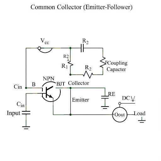
Great! Now, let's look at the circuit diagram. Notice how the collector terminal isn't at AC ground, which is crucial for our analysis.

Why is it important that it's not at AC ground?
Good question! This allows for signal development at the collector terminal, affecting our calculations for the output voltage. We'll see how this plays into our voltage gain formula in later sections.
Voltage Gain in Amplifiers
🔒 Unlock Audio Lesson
Sign up and enroll to listen to this audio lesson

Let's shift our focus to calculating voltage gain. Can anyone express the formula for voltage gain in our amplifier?

Is it just \( A_v = \frac{V_o}{V_{in}} \)?
Perfect! However, remember that in the case of our Common Collector, the gain \( A_v \) is approximately 1. Can someone explain why that is?

Because the output voltage is almost the same as the input voltage?
Exactly! This is characteristic of a buffer, helping us maintain the original signal without loss. Let's reinforce that understanding: what happens if we connect a load at the output?
It might pull down the output voltage a bit!
Correct! Thus maintaining high input and low output impedance remains crucial for the performance of the amplifier.
Input and Output Resistance
🔒 Unlock Audio Lesson
Sign up and enroll to listen to this audio lesson
Now, let's evaluate input and output resistances. Who can tell me the significance of having high input resistance in our circuits?
It prevents loading the previous stage, ensuring we get accurate signals, right?
Exactly! High input resistance allows our circuits to interact without affecting the source signal. Now, how about output resistance? Why is it kept low?
To drive loads more effectively without dropping voltage?
Spot on! The goal is to maximize signal transfer to the load. We can derive these resistances using our open circuit parameters, leading to the formula we established earlier. Can anyone summarize what affects these resistances?
The resistances added at the collector terminal and the transistor parameters play a role?
Well said! This relationship is foundational for understanding amplifier behavior.
Capacitance Effects
🔒 Unlock Audio Lesson
Sign up and enroll to listen to this audio lesson
Let's delve into input capacitance next. What can you tell me about the Miller Effect and its implications for input capacitance?
Isn't it where the capacitance effectively looks larger due to feedback?
Absolutely right! This phenomenon affects the input capacitance of our amplifier significantly. Can anyone think of how it applies specifically to our circuit?
You mean the capacitance looking like it's amplified, making it harder for higher frequencies to pass?
Exactly! This leads us to note that for high frequencies, the performance can degrade due to these increased capacitances. Remember – high-frequency behavior is often influenced by both physical and effective capacitances.
So, in designing these amplifiers, we need to consider capacitance values carefully?
Yes! The effective capacitance must be taken into account to predict and optimize performance accurately.
Introduction & Overview
Read summaries of the section's main ideas at different levels of detail.
Quick Overview
Standard
The section provides a comprehensive overview of Common Collector and Common Drain amplifier analyses, detailing the relationships between input and output voltages, resistances, and their impacts on circuit performance. Key parameters including voltage gain, input resistance, and output resistance are elaborated upon using circuit analysis techniques.
Detailed
Complex Circuit Analysis
This section focuses on the analysis of Common Collector and Common Drain amplifiers in the context of analog electronic circuits. It delves into the voltage gain, input resistance, and output resistance, crucial for understanding the performance characteristics of these amplifiers.
Key Concepts Covered:
- Common Collector Amplifier: The section introduces the Common Collector amplifier, emphasizing its configuration and significance in circuit analysis. The voltage drops at various terminals are calculated to determine the overall behavior of the amplifier.
- Key point: Understanding that the collector terminal does not act as an AC ground but retains a signal value.
- Voltage Gain Calculation: The relation between input voltage ($v_{in}$) and output voltage ($v_{o}$) is discussed, highlighting that $v_{o}$ tends to approximate $v_{in}$ in value, resulting in a voltage gain close to 1 under certain conditions.
- Key point: Voltage gain $v_{o} = v_{in} imes G$, where G is close to 1, indicating a buffer behavior of the amplifier.
- Input and Output Resistance: The section analyzes input and output resistances, demonstrating how they change with the inclusion of resistances at the collector terminal. Input resistance is shown to potentially increase due to added resistances in series.
- Key point: Input resistance is significantly high, while output resistance remains relatively low.
- Capacitance Implications: The analysis addresses the input capacitance and its dependency on feedback effects. Two capacitance components are considered and their contributions are calculated to derive the overall input capacitance.
- Key point: Input capacitance trends lower due to Miller effect interactions.
In summary, this section employs circuit analysis techniques to reveal insights into the operational characteristics of Common Collector and Common Drain amplifiers, laying the groundwork for further exploration into circuit design and analysis.
Youtube Videos

Audio Book
Dive deep into the subject with an immersive audiobook experience.
Introduction to Common Collector Amplifier
Chapter 1 of 5
🔒 Unlock Audio Chapter
Sign up and enroll to access the full audio experience
Chapter Content
Yeah, welcome back after the short break and we are discussing about the Common Collector Amplifier, considering the; considering the resistance R connected in the collector terminal in between collector and supply voltage Vdd.
Detailed Explanation
The discussion begins by reintroducing the Common Collector Amplifier (CCA). This type of amplifier configuration is noted for its ability to provide high input impedance and low output impedance, making it useful as a voltage buffer. The setup involves a resistor (R) connected between the collector terminal and the supply voltage (Vdd), which is crucial for the amplifier's function. This setup allows for a more refined analysis of how signals are transmitted through the circuit.
Examples & Analogies
Think of the Common Collector Amplifier as a bridge in a city. The people (signals) can enter the bridge (input terminal) at one end and exit at the other while experiencing minimal resistance (impedance). The bridge doesn’t complicate the flow of people; it allows them to cross easily without significant increase in difficulty, much like how the CCA allows signals to pass through while maintaining their integrity.
Input and Output Relationships
Chapter 2 of 5
🔒 Unlock Audio Chapter
Sign up and enroll to access the full audio experience
Chapter Content
So, we do have the collector terminal which is not AC ground rather it may be having a signal called say vc. So, this is very important change compared to our previous analysis.
Detailed Explanation
In this section, the significance of the collector terminal being non-AC ground is emphasized. Unlike previous analyses where certain terminals might be assumed to be at ground potential, here the collector terminal can have an actual signal (vc). This change is essential as it affects how the input and output signals are interpreted within the circuit. We can visualize that the output voltage (vo) is influenced directly by the collector current as it is linked to the base current (ib). There is a reciprocal relationship established between these elements, forming the basis for voltage gain calculations.
Examples & Analogies
Imagine a teacher (the base signal) who connects with students (the collector signal). If the teacher changes their volume or tone while speaking (the AC signal), the students respond based on what they understand without getting confused with background noise (AC ground). The interaction reinforces the message, illustrating how the collector's signal adds depth to the circuit's function, similar to how vocal variations deepen communication.
Applying Kirchhoff's Current Law
Chapter 3 of 5
🔒 Unlock Audio Chapter
Sign up and enroll to access the full audio experience
Chapter Content
So, we can say that the current flow after reaching to the emitter whether it is branching to the active device or through this Rc; finally, they are converging to the ground.
Detailed Explanation
Applying Kirchhoff's Current Law (KCL) helps analyze the current flowing in the circuit. The current reaching the emitter can branch off to either the active device or through the collector resistor (Rc). Ultimately, these currents combine and converge to ground. This convergence can help us understand how base current (ib) relates to other circuit variables, allowing for a clearer analysis of current flow.
Examples & Analogies
Consider a water pipeline system. The water (current) flows through various branches and divides among different pathways (active device or Rc). Eventually, all pathways lead back to the reservoir (ground). Understanding the flow of water helps us manage our supply effectively, similar to how analyzing current branches aids in optimizing circuit performance.
Voltage Gain Calculation
Chapter 4 of 5
🔒 Unlock Audio Chapter
Sign up and enroll to access the full audio experience
Chapter Content
Now, if we rearrange that equation, what we will be getting is vo = vi(k).
Detailed Explanation
The analysis leads to a formulation of the voltage gain, expressed as the relationship between output voltage (vo) and input voltage (vi). By utilizing previously derived equations, we can deduce that the voltage gain k is very close to unity (1), indicating that the output voltage closely resembles the input voltage.
Examples & Analogies
Imagine a very efficient speaker that barely distorts the sound signals it receives. When you play a song on the speaker, the sound output (vo) is almost identical to the original music track (vi), showcasing high fidelity. This is akin to the voltage gain in the CCA, where the output effectively matches the input, providing clear amplification without distortion.
Understanding Resistance and Impedance
Chapter 5 of 5
🔒 Unlock Audio Chapter
Sign up and enroll to access the full audio experience
Chapter Content
We do have let us move to the next slide to do that.
Detailed Explanation
The discussion transitions into examining input resistance and overall circuit impedance. It describes how input resistance, particularly when considering resistances in series and their contributions to overall impedance, affects input characteristics and hence signal behavior in the circuit.
Examples & Analogies
Consider a traffic system where different roads (resistors) converge into a main highway (overall impedance). If one road is narrow (high resistance), it affects the flow of traffic on the highway, just like high resistance affects input characteristics. Understanding the way roads merge can help optimize travel time and reduce congestion, similar to how analyzing resistance aids in managing circuit performance.
Key Concepts
-
Common Collector Amplifier: The section introduces the Common Collector amplifier, emphasizing its configuration and significance in circuit analysis. The voltage drops at various terminals are calculated to determine the overall behavior of the amplifier.
-
Key point: Understanding that the collector terminal does not act as an AC ground but retains a signal value.
-
Voltage Gain Calculation: The relation between input voltage ($v_{in}$) and output voltage ($v_{o}$) is discussed, highlighting that $v_{o}$ tends to approximate $v_{in}$ in value, resulting in a voltage gain close to 1 under certain conditions.
-
Key point: Voltage gain $v_{o} = v_{in} imes G$, where G is close to 1, indicating a buffer behavior of the amplifier.
-
Input and Output Resistance: The section analyzes input and output resistances, demonstrating how they change with the inclusion of resistances at the collector terminal. Input resistance is shown to potentially increase due to added resistances in series.
-
Key point: Input resistance is significantly high, while output resistance remains relatively low.
-
Capacitance Implications: The analysis addresses the input capacitance and its dependency on feedback effects. Two capacitance components are considered and their contributions are calculated to derive the overall input capacitance.
-
Key point: Input capacitance trends lower due to Miller effect interactions.
-
-
In summary, this section employs circuit analysis techniques to reveal insights into the operational characteristics of Common Collector and Common Drain amplifiers, laying the groundwork for further exploration into circuit design and analysis.
Examples & Applications
In a Common Collector amplifier with a collector resistance of 1kΩ, the input voltage is 2V, and the output voltage is measured at 1.95V, illustrating a voltage gain close to 1.
An amplifier circuit designed with very high input resistance (e.g., 100kΩ) may have an output resistance of 500Ω, allowing it to drive heavier loads effectively.
Memory Aids
Interactive tools to help you remember key concepts
Rhymes
In the Common Collector's domain, high in, low out is the gain.
Stories
Imagine a stream flowing through a pipe. If the pipe is wide at the entrance and narrow at the exit, the flow stays steady. This illustrates how a Common Collector keeps the voltage steady while powering a load.
Memory Tools
Remember VALVE: V for Voltage Gain, A for Amplifier Type, L for Low Output, V for Variable Load, E for Effective Resistance.
Acronyms
Use the acronym 'CIVIL' to remember
for Common Collector
for Input Impedance high
for Voltage Gain around 1
for Input Resistance high
and L for Low Output Resistance.
Flash Cards
Glossary
- Voltage Gain
The ratio of output voltage to input voltage, indicating the amplification level in a circuit.
- Common Collector
An amplifier configuration that provides a high input impedance and a low output impedance.
- Input Resistance
The resistance seen by a signal source connected to the input of a circuit.
- Output Resistance
The resistance at the output terminals of a circuit facing the load.
- Miller Effect
An increase in input capacitance due to feedback in amplifiers, affecting bandwidth and frequency response.
Reference links
Supplementary resources to enhance your learning experience.