
CMOS Inverter Operation
Enroll to start learning
You’ve not yet enrolled in this course. Please enroll for free to listen to audio lessons, classroom podcasts and take practice test.
Interactive Audio Lesson
Listen to a student-teacher conversation explaining the topic in a relatable way.
Operation of the CMOS Inverter
🔒 Unlock Audio Lesson
Sign up and enroll to listen to this audio lesson

Let's start with the basics of the CMOS inverter operation. Can anyone tell me what happens when the input is high?

The NMOS turns on and the PMOS turns off!
Exactly! And can someone explain what the output will be when this happens?

The output will be low, or 0!
Correct! So remember, we can use the acronym 'HIN' - High Input, NMOS ON, Output Low. Now, what happens when the input is low?

The PMOS turns on and the NMOS turns off, pulling the output high!
Right! We can remember this with 'LIN' - Low Input, PMOS ON, Output High. Understanding these transitions is fundamental for CMOS designs. To recap: HIN and LIN help visualize how inputs affect outputs.
Power Consumption in CMOS Inverters
🔒 Unlock Audio Lesson
Sign up and enroll to listen to this audio lesson

Now, let's discuss something very important – power consumption in CMOS inverters. Why do you think it's crucial to minimize power usage?

To extend battery life in portable devices and reduce heat generation!
Exactly! Since at any time only one transistor is active, this minimizes static power consumption. Can anybody connect this to real-world applications?
In mobile phones or laptops, low power consumption means better battery life!
Precisely! Always remember that CMOS technology is preferred in battery-operated devices for this reason. This operational efficiency is why we favor CMOS in digital circuits.
Practical Applications of CMOS Inverters
🔒 Unlock Audio Lesson
Sign up and enroll to listen to this audio lesson
Finally, let’s discuss where we use CMOS inverters in real life. Can anyone name some applications?
They are used in microprocessors and digital logic circuits!
Great examples! They're integral in various applications, such as memory devices, which all require efficient signal inversion. How do we ensure these devices remain efficient?
By optimizing the switching speed and minimizing power waste!
Exactly! Efficiency in CMOS inverters allows for high-performance computing while safeguarding power. Remember, their role extends beyond simple signal inversion; they are foundational to modern electronics.
Introduction & Overview
Read summaries of the section's main ideas at different levels of detail.
Quick Overview
Standard
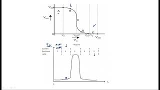
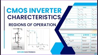
In this section, we explore the operation of the CMOS inverter, which utilizes NMOS and PMOS transistors. The inverter toggles its output based on high or low input signals, thereby pulling the output high or low while achieving low static power consumption due to the complementary operation of its transistors.
Detailed
CMOS Inverter Operation
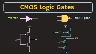
The CMOS inverter is a fundamental component of CMOS technology, characterized by its use of both NMOS and PMOS transistors. The operation is simple yet effective: when a high input (1) is applied, the NMOS transistor conducts, pulling the output voltage down to 0, while simultaneously, the PMOS transistor is off. Conversely, when a low input (0) is provided, the PMOS transistor turns on, pulling the output high to 1, and the NMOS transistor turns off. This complementary action ensures that only one transistor conducts at any given time, resulting in very low static power consumption, critical for efficient design in modern integrated circuits.
Youtube Videos
Audio Book
Dive deep into the subject with an immersive audiobook experience.
Input High State
Chapter 1 of 3
🔒 Unlock Audio Chapter
Sign up and enroll to access the full audio experience
Chapter Content
● Input High (1): When the input is high, the NMOS transistor turns on, pulling the output low (0). At the same time, the PMOS transistor turns off.
Detailed Explanation
In a CMOS inverter, when the input signal is high (represented as '1'), the NMOS transistor becomes active or 'on'. This means it conducts electricity and allows current to flow from the drain to the source. Because this action pulls the output to a low state (0), it effectively connects the output to ground (0V). Conversely, during this state, the PMOS transistor is turned off, preventing any current from flowing through it. This complementary action between the NMOS and PMOS transistors is what enables the inverter to function correctly.
Examples & Analogies
Think of the CMOS inverter like a seesaw in a playground. When one side (NMOS) goes up (turns on), the other side (PMOS) goes down (turns off), resulting in a downward motion that signifies '0'. This dynamic balance between the two keeps the seesaw (output) stable depending on which side is activated.
Input Low State
Chapter 2 of 3
🔒 Unlock Audio Chapter
Sign up and enroll to access the full audio experience
Chapter Content
● Input Low (0): When the input is low, the PMOS transistor turns on, pulling the output high (1). The NMOS transistor turns off.
Detailed Explanation
When the input to the CMOS inverter is low (represented as '0'), the PMOS transistor is turned on. This means it conducts current from the power supply to the output, effectively pulling the output voltage up to high (1). Simultaneously, the NMOS transistor turns off, preventing any current from passing through it. This operation illustrates the inverter's complementary nature: while one transistor is on, the other is off, ensuring that the output is definitively at a high state.
Examples & Analogies
Returning to our seesaw analogy, when the NMOS side is down (off), the PMOS side goes up (on), lifting the seesaw. This action results in the seesaw (output) being elevated to signify '1'. Just like two opposing players on a seesaw, they cannot be up or down at the same time, ensuring a clear signal output.
Power Consumption
Chapter 3 of 3
🔒 Unlock Audio Chapter
Sign up and enroll to access the full audio experience
Chapter Content
● Power Consumption: The CMOS inverter has very low static power consumption since only one transistor is conducting at a time, resulting in minimal current flow.
Detailed Explanation
One of the significant advantages of a CMOS inverter is its low static power consumption. This occurs because, during operation, only one of the transistors (either NMOS or PMOS) is active at any given moment. When one transistor conducts, the other is off, leading to negligible current flow in the circuit. As a result, there’s very little power wasted as heat, making CMOS technology particularly energy-efficient, especially for portable and battery-powered applications.
Examples & Analogies
Imagine a light switch that only allows current to pass when it is flipped up or down but never both at the same time. This design means that when the light is off, no electricity flows, and when it’s on, it operates efficiently. Similarly, the CMOS inverter efficiently switches between states without unnecessary energy use.
Key Concepts
-
CMOS Inverter: A fundamental circuit that uses NMOS and PMOS transistors to perform logic inversion.
-
Complementary Operation: An operational mode where one transistor turns off while the other turns on, ensuring low static power consumption.
-
Static Power Consumption: The power consumed when the inverter is idle, minimized in a CMOS inverter.
Examples & Applications
A smartphone uses CMOS inverters in its processor to combine low power consumption with high performance.
Digital logic gates in computers use CMOS inverters to manage signal levels efficiently.
Memory Aids
Interactive tools to help you remember key concepts
Rhymes
In logic gates of CMOS might, NMOS pulls low, while PMOS pulls high.
Stories
Imagine two friends, NMOS and PMOS, where NMOS loves to go low and PMOS enjoys being high. They work together to help devices be efficient.
Memory Tools
Remember HIN for High Input and NMOS ON, and LIN for Low Input and PMOS ON.
Acronyms
HIN
High Input
NMOS on
Inverter Low.
Flash Cards
Glossary
- CMOS Inverter
A circuit that inverts the input signal using complementary NMOS and PMOS transistors, characterized by low power consumption.
- NMOS Transistor
A type of MOSFET that conducts when a positive voltage is applied to the gate, commonly used in CMOS circuits.
- PMOS Transistor
A type of MOSFET that conducts when the gate voltage is lower than the source voltage, used complementarily with NMOS in CMOS circuits.
- Static Power Consumption
Power consumed by a circuit when not switching, which is minimized in CMOS inverters as only one transistor is on at a time.
- Threshold Voltage
The minimum gate voltage required to turn on a MOSFET; critical for the switching operation of NMOS and PMOS transistors.
Reference links
Supplementary resources to enhance your learning experience.