
Characteristics and Behavior of CMOS Devices
Enroll to start learning
You’ve not yet enrolled in this course. Please enroll for free to listen to audio lessons, classroom podcasts and take practice test.
Interactive Audio Lesson
Listen to a student-teacher conversation explaining the topic in a relatable way.
Introduction to NMOS and PMOS Devices
🔒 Unlock Audio Lesson
Sign up and enroll to listen to this audio lesson

Today we're discussing the fundamental building blocks of CMOS technology: NMOS and PMOS transistors. Can anyone explain how NMOS works?

NMOS transistors conduct when a positive voltage is applied to the gate, right?
Exactly! This condition is specified by the threshold voltage, or Vth. Remember, once the gate-source voltage surpasses Vth, the NMOS turns on. Let’s say it together: 'Above Vth, NMOS is alive!' What's the opposite behavior for PMOS?

PMOS works with a negative voltage applied to the gate, so it conducts when VGS is less than Vth.
Correct! Remember: 'Negative Vth makes PMOS connect.' Great job, everyone!
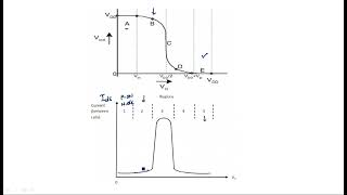
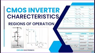
Operating Regions of NMOS and PMOS
🔒 Unlock Audio Lesson
Sign up and enroll to listen to this audio lesson

Now, let’s explore the operation regions of NMOS. Who can tell me about the cutoff region?

In the cutoff region, if VGS is below Vth, the NMOS transistor is off, and no current flows.
Great! Shift to the linear region, how does the NMOS behave there?

It acts like a resistor, and the current flows linearly with VDS.
Spot on! In the saturation region, however, the current is controlled by VGS and not really by VDS. What can you tell me about the PMOS regions?
PMOS has the same regions as NMOS, cutoff, linear, and saturation, but it conducts with negative gate voltage.
Exactly! Let’s recap what we learned: Cutoff means off, linear means like a resistor, and saturation means currents vary with VGS. Excellent work!
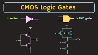
CMOS Inverter Functionality
🔒 Unlock Audio Lesson
Sign up and enroll to listen to this audio lesson
Moving on to our CMOS inverter! Who can describe how it functions when the input is high?
When the input is high, the NMOS turns on and pulls the output low.
Fantastic! And what happens when the input is low?
The PMOS turns on and pulls the output high, while the NMOS is off.
Correct again! Minimal static power consumption is a major advantage here since only one transistor is active at any time. Let’s remember: 'In CMOS, one active, one inactive; energy is conserved!'
Threshold Voltage and Variations
🔒 Unlock Audio Lesson
Sign up and enroll to listen to this audio lesson
Threshold voltage is a critical aspect of our MOSFETs. Can anyone share why its variations matter?
Variations in Vth can affect when the transistor turns on, yes?
Exactly! Factors like process variations, temperature changes, and bias effects can all lead to shifts in Vth. How can these affect the performance of our circuits?
If Vth is too high, the transistor might not turn on properly, causing issues in digital circuits.
Great insight! Understanding these variations is essential for reliability in CMOS designs. Let’s keep that in mind: 'Vth’s truth, high or low, affects our flow!'
Channel-Length Modulation
🔒 Unlock Audio Lesson
Sign up and enroll to listen to this audio lesson
Today, let’s tackle channel-length modulation. Does anyone know what this phenomenon means?
It happens when the effective length of the conductive channel changes with VDS, right?
Exactly! And why is this particularly significant in short-channel devices?
Because it can affect current flow, and in short channels, the effect becomes more pronounced!
Correct! Let’s summarize: Channel-length modulation impacts current in saturation, especially noticeable in short-channel devices where λ becomes important. Remember: 'Long channels, small changes; short channels, big impacts!'
Introduction & Overview
Read summaries of the section's main ideas at different levels of detail.
Quick Overview
Standard
This section delves into the operation of CMOS devices, emphasizing NMOS and PMOS transistors, their voltage thresholds, current characteristics, and the configuration of CMOS inverters, highlighting their significance in low-power applications.
Detailed
Characteristics and Behavior of CMOS Devices
CMOS (Complementary Metal-Oxide-Semiconductor) devices are crucial in the realm of integrated circuits (ICs), primarily functioning through NMOS (n-channel) and PMOS (p-channel) transistors. These transistors embody complementary properties that minimize static power consumption, operating in a way wherein one is on while the other is off. The NMOS transistor conducts when its gate-source voltage exceeds the threshold (Vth), illustrating operation through regions such as cutoff, linear/ohmic, and saturation. The I-V characteristics reflect these behaviors, with varying drain current influenced by voltage changes.
Conversely, PMOS transistors operate oppositely, requiring a negative gate-source voltage for conduction, and their behaviors also include similar operating regions. Furthermore, the CMOS inverter demonstrates the fundamental application of these transistors, highlighting energy efficiency by ensuring that only one transistor is active at any time, thus minimizing power flow during operation. The section also introduces vital concepts like channel-length modulation effects and the significance of threshold voltage variations, essential for modern circuit design and reliability.
Youtube Videos
Audio Book
Dive deep into the subject with an immersive audiobook experience.
Introduction to CMOS Devices
Chapter 1 of 5
🔒 Unlock Audio Chapter
Sign up and enroll to access the full audio experience
Chapter Content
CMOS (Complementary Metal-Oxide-Semiconductor) devices are the building blocks of modern integrated circuits (ICs), particularly for logic gates, memory devices, and signal processing systems. CMOS technology relies on the use of NMOS (n-channel metal-oxide-semiconductor) and PMOS (p-channel metal-oxide-semiconductor) transistors, which are complementary to each other. The behavior and characteristics of these devices are essential for understanding CMOS circuit design and performance.
Detailed Explanation
CMOS devices are vital components used in modern electronic circuits such as computers and smartphones. They consist of two types of transistors: NMOS and PMOS, which work in harmony to perform various logic functions. Understanding how these transistors operate and interact is critical for designing effective circuits. NMOS and PMOS transistors complement each other, meaning that while one is on (allowing current to pass), the other is off, which helps in minimizing energy consumption. This section emphasizes the importance of CMOS technology in the functionality of integrated circuits.
Examples & Analogies
Think of a light switch in a room. When one switch is turned on, the light is on, and the other switch is off, leading to no energy waste when the light is off. Similarly, in CMOS devices, when one type of transistor allows electrical current to flow, the other type is turned off, ensuring that no unnecessary power is consumed.
Basic Operation of NMOS and PMOS Transistors
Chapter 2 of 5
🔒 Unlock Audio Chapter
Sign up and enroll to access the full audio experience
Chapter Content
The operation of CMOS devices is based on the interaction between NMOS and PMOS transistors. These devices are designed to operate in complementary modes, meaning when one transistor is on, the other is off, ensuring minimal static power consumption.
Detailed Explanation
In CMOS technology, both NMOS and PMOS transistors are used together to ensure efficient operation. The complementary nature of these transistors allows for effective switching with low power consumption. This means that at any given time, either the NMOS or PMOS is in the 'on' state, while the other is turned 'off,' preventing current flow and thus reducing wasted energy. This approach is fundamental to the design of CMOS circuits.
Examples & Analogies
Imagine a bicycle powered by two pedals: when one pedal is pushed down, the other is lifted up. This efficient movement means that energy is not wasted by having both pedals pedal at the same time. In CMOS technology, this similar principle is applied to the NMOS and PMOS transistors, maintaining low power usage.
NMOS Transistor Behavior
Chapter 3 of 5
🔒 Unlock Audio Chapter
Sign up and enroll to access the full audio experience
Chapter Content
An NMOS transistor has an n-type channel that conducts current when a positive voltage is applied to the gate relative to the source (known as gate-source voltage, or VGSV_{GS}).
Detailed Explanation
NMOS transistors function when a positive voltage is applied to their gate, which creates a conductive channel allowing current to flow from the drain to the source. The amount of current flow depends on the gate-source voltage; if this voltage exceeds a particular level known as the threshold voltage, the transistor turns 'on.' This section describes the three main operational regions of NMOS transistors: the cutoff region (off state), the linear region (acting like a variable resistor), and the saturation region (where the transistor is fully on).
Examples & Analogies
Consider a water faucet: when you turn the handle (application of voltage), water starts to flow. If you turn it a little, the water trickles (linear region), and if you turn it fully, the water flows freely (saturation region). In this analogy, the faucet is like the NMOS transistor, with the handle representing the gate voltage.
PMOS Transistor Behavior
Chapter 4 of 5
🔒 Unlock Audio Chapter
Sign up and enroll to access the full audio experience
Chapter Content
A PMOS transistor has a p-type channel and is controlled by a negative gate-source voltage. The PMOS transistor conducts current when the gate voltage is lower than the source voltage (i.e., VGS
Detailed Explanation
PMOS transistors operate in a manner that is complementary to NMOS transistors. They require a negative gate-source voltage to allow current to flow from the source to the drain. This section also outlines the similar operational regions as NMOS: cutoff (off state), linear (acting as a resistor), and saturation (fully on). Understanding PMOS behavior is essential for integrating them into CMOS circuits.
Examples & Analogies
If we return to the water analogy: think of the faucet again but now imagine it requires a push down to open it. When you push down hard enough (negative voltage), water flows (current conducts). Like the PMOS transistor, which opens when the input (or gate voltage) is lower than a certain level.
CMOS Inverter and its Behavior
Chapter 5 of 5
🔒 Unlock Audio Chapter
Sign up and enroll to access the full audio experience
Chapter Content
The CMOS inverter is one of the most fundamental CMOS circuits. It uses both NMOS and PMOS transistors in a complementary configuration to invert the input signal.
Detailed Explanation
A CMOS inverter is a critical building block in digital circuits. It takes a single input and produces an output that is the opposite of the input; for example, if you input a high signal (1), the output will be low (0). This inversion is achieved through the complementary action of NMOS and PMOS transistors: when one is on, the other is off. The inverter also boasts low power consumption since only one transistor conducts at any time.
Examples & Analogies
Think of a seesaw in a playground: when one side goes up, the other side goes down. Just like the inverter, pushing one end (high input) causes the opposite end (output) to go low. It's a balance that leads to a clear, low-energy way to manage electronic signals.
Key Concepts
-
NMOS and PMOS are complementary transistors vital for CMOS technology.
-
The functioning of CMOS relies on threshold voltage (Vth) for switching behavior.
-
CMOS inverters are fundamental for realizing digital logic circuits in a power-efficient way.
-
Channel-length modulation affects drain current, especially in short-channel devices.
Examples & Applications
Example: A CMOS inverter receives a high input (1), activating the NMOS to output low (0). When the input is low (0), the PMOS is activated, outputting high (1).
Example: In temperature-sensitive applications, if the temperature rises, the threshold voltage decreases, which might cause an NMOS transistor to turn on under unintended circumstances.
Memory Aids
Interactive tools to help you remember key concepts
Rhymes
NMOS is positive, PMOS is negative, switch on the right voltage and let them revel in.
Stories
Imagine a seesaw: NMOS and PMOS are on opposite sides. Only one can be up while the other is down, balancing out energy like in circuits.
Memory Tools
Remember 'C-L-S' for NMOS: Cutoff, Linear, Saturation.
Acronyms
Use 'V-GS' to recall Gate-Source Voltage critical for transistor operation.
Flash Cards
Glossary
- CMOS
A technology for constructing integrated circuits using complementary pairs of p-type and n-type MOSFETs.
- NMOS Transistor
A type of MOSFET that conducts when a positive voltage is applied to the gate.
- PMOS Transistor
A type of MOSFET that conducts when a negative voltage is applied to the gate.
- Threshold Voltage (Vth)
The minimum gate-source voltage needed to create a conductive channel in a MOSFET.
- Saturation Region
An operational state where the current is primarily controlled by the gate-source voltage and is relatively independent of drain-source voltage.
- ChannelLength Modulation
A phenomenon where the effective channel length of a MOSFET changes with the applied drain-source voltage.
- Inverter
A basic CMOS circuit configuration that outputs the opposite logic level of its input.
Reference links
Supplementary resources to enhance your learning experience.