
Emerging Technologies in Compound Semiconductors
Interactive Audio Lesson
Listen to a student-teacher conversation explaining the topic in a relatable way.
Introduction to Compound Semiconductors
🔒 Unlock Audio Lesson
Sign up and enroll to listen to this audio lesson

Today, we will discuss compound semiconductors, starting with their unique properties. Who can tell me what makes these semiconductors special?

They have wide bandgaps, which allows for higher efficiency and power capabilities, right?
Correct! These properties indeed enable operations at higher frequencies and voltages compared to silicon. Remember the acronym WBG - Wide Bandgap, it helps in recalling these concepts.

What about the applications? Where are these materials used?
Great question! WBG materials like GaN and SiC are used in power electronics and RF applications. This leads us to our next topic on applications.
Emerging Applications of Compound Semiconductors
🔒 Unlock Audio Lesson
Sign up and enroll to listen to this audio lesson

Now let's delve into the applications of these materials. How about we start with wireless technology?

Isn't 5G relying a lot on GaN HEMTs for its infrastructure?
Exactly! GaN HEMTs play a crucial role in massive MIMO systems for 5G. Can anyone explain what massive MIMO means?

It stands for multiple input multiple output, which helps in transmitting data simultaneously to multiple users!
Perfect! This technology enables high-bandwidth data transmission, crucial for today’s demanding applications.
Recent Innovations and Challenges
🔒 Unlock Audio Lesson
Sign up and enroll to listen to this audio lesson
Let's move to recent innovations. Can anyone name a recent method of fabrication for compound semiconductors?
I heard about GaN-on-Diamond substrates? They help with thermal management.
Correct! This method greatly enhances the performance of high-power RF applications. But what challenges do we still face?
There's the high cost of materials and integration issues, right?
Exactly! Tackling these challenges is key for future advancements in the field.
Market Trends and Future Directions
🔒 Unlock Audio Lesson
Sign up and enroll to listen to this audio lesson
Finally, let's look at market trends. What do we predict for the compound semiconductor market in the coming years?
It’s forecasted to exceed $150 billion by 2030, right?
Absolutely! Aerospace, telecom infrastructure, and renewable energy are key sectors driving this market growth. Can anyone think of why renewable energy would be significant?
Because we need efficient power conversion technologies for renewable sources?
Great insight! Efficiency in energy conversion is vital for sustainable energy solutions.
Introduction & Overview
Read summaries of the section's main ideas at different levels of detail.
Quick Overview
Standard
Compound semiconductors play a crucial role in various advanced technologies, including telecommunications, renewable energy, and quantum computing. This section discusses key innovations such as wide bandgap materials and their application advantages, as well as ongoing challenges and advancements in the field.
Detailed
Emerging Technologies in Compound Semiconductors
Compound semiconductors are revolutionizing multiple industries, particularly telecommunications, renewable energy, quantum computing, and autonomous systems. Their inherent characteristics, including wide bandgap, high breakdown voltage, and direct bandgap, provide capabilities that traditional silicon-based semiconductors cannot match.
Problem Statement
Compound semiconductors facilitate significant breakthroughs in various next-generation technologies, and the chapter investigates recent advancements impacting research, fabrication, and integration.
Key Emerging Materials and Trends
-
Wide Bandgap (WBG) and Ultra-Wide Bandgap (UWBG) Semiconductors
Materials include GaN, SiC, and diamond, which support elevated voltage, frequency, and temperature operations leading to more compact and efficient devices. -
2D and Nanostructured Compound Semiconductors
Examples like InSe and GaSe enable flexible and transparent electronics suitable for wearable sensors and neuromorphic computing. -
Heterogeneous Integration with Silicon
Integrating CMOS with III-V semiconductors allows for diverse functionalities on a single chip, showcasing platforms like GaN-on-Si and GaAs-on-SOI.
Advanced Applications Enabled by Compound Semiconductors
- Wireless Systems (5G and 6G): GaN HEMTs are vital for efficient massive MIMO antennas, while InP and GaAs ICs enable mmWave transceivers.
- Electric Vehicles and Smart Grids: SiC MOSFETs and GaN transistors contribute to reduced inverter size and enhanced efficiency.
- Quantum and Neuromorphic Computing: InAs/GaSb quantum wells are explored for topological qubits, enhancing computing capabilities.
- LiDAR and 3D Sensing: Utilizing VCSELs in autonomous technologies facilitates depth sensing and mapping.
Recent Innovations in Fabrication and Integration
Innovative methods such as GaN-on-Diamond for thermal management and wafer bonding to silicon platforms are advancing integration processes.
Market Trends and Industrial Momentum
The compound semiconductor market is projected to surpass $150 billion by 2030, with key sectors including aerospace, renewable energy, and telecom infrastructure driving growth.
Challenges and Research Directions
Identified challenges include high fabrication costs and material defects, prompting research towards scalable and sustainable solutions.
Conclusion
With their unique properties and capabilities, compound semiconductors are positioned to lead the advancements in various future technologies, making them essential to the evolution of modern electronics.
Youtube Videos
Audio Book
Dive deep into the subject with an immersive audiobook experience.
Introduction to Compound Semiconductors
Chapter 1 of 4
🔒 Unlock Audio Chapter
Sign up and enroll to access the full audio experience
Chapter Content
Compound semiconductors are at the forefront of innovation across diverse sectors, including telecommunications, renewable energy, quantum computing, and autonomous systems. Their unique physical properties—such as wide bandgap, high breakdown voltage, and direct bandgap—enable device capabilities beyond what silicon alone can offer. This chapter explores the latest developments and future trends in compound semiconductor technologies and highlights emerging applications that are shaping the next generation of electronic, photonic, and energy systems.
Detailed Explanation
The introduction provides an overview of what compound semiconductors are and why they are important. Unlike traditional silicon semiconductors, compound semiconductors are made from two or more elements, which gives them unique properties. For instance, their wide bandgap allows them to operate at higher temperatures and voltages compared to silicon. This makes them ideal for advanced applications such as telecommunications, renewable energy sources, and even technologies like quantum computing. The chapter aims to discuss recent advancements in these materials and how they are being utilized across various innovative fields.
Examples & Analogies
Imagine if traditional cars (silicon semiconductors) could only run at a specific speed and under certain conditions, but then you discover a new type of vehicle (compound semiconductors) that can race under extreme weather conditions and on rugged terrains. That’s how compound semiconductors provide significant enhancements over regular semiconductors!
Key Emerging Materials and Trends
Chapter 2 of 4
🔒 Unlock Audio Chapter
Sign up and enroll to access the full audio experience
Chapter Content
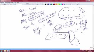
Wide Bandgap (WBG) and Ultra-Wide Bandgap (UWBG) Semiconductors
| - Material | Bandgap (eV) | Applications |
|---|---|---|
| GaN | ~3.4 | RF, power electronics, 5G |
| SiC | ~3.3 | EV inverters, power conversion |
| Diamond | ~5.5 | High-power electronics (R&D) |
| Ga₂O₃ | ~4.8 | Low-cost high-voltage switches |
| AlN | ~6.2 | Deep UV LEDs, RF components |
| - Enable higher voltage, frequency, and temperature operation than traditional semiconductors. | ||
| - Lead to smaller, more efficient, and more reliable power and RF devices. |
Detailed Explanation
This section focuses on the emergence of wide bandgap (WBG) and ultra-wide bandgap (UWBG) semiconductors. These materials have a bandgap significantly larger than silicon, allowing them to operate at higher voltages and temperatures. For instance, Gallium Nitride (GaN) is widely used in 5G technology due to its ability to handle high power and frequency. The benefits of using these materials include enhanced efficiency, smaller device sizes, and improved reliability in high-performance applications.
Examples & Analogies
Think of it like using a special tank to store water under high pressure; traditional materials might burst under that pressure, but these advanced materials are like reinforced tanks that can hold even more water without bursting, which in the tech world translates to more powerful devices.
2D and Nanostructured Compound Semiconductors
Chapter 3 of 4
🔒 Unlock Audio Chapter
Sign up and enroll to access the full audio experience
Chapter Content
2D and Nanostructured Compound Semiconductors
- Examples: InSe, GaSe, MoS₂-based heterostructures
- Advantages:
- Atomic-scale thickness → quantum confinement
- Flexible, transparent electronics
- Applications: Wearable sensors, neuromorphic computing, flexible displays.
Detailed Explanation
2D and nanostructured compound semiconductors are incredibly thin materials that can be just a few atoms thick. This atomic-scale thickness allows these materials to exhibit quantum effects, which can be exploited in advanced technologies. Their flexibility and transparency make them suitable for applications in wearable sensors, which track health metrics, and neuromorphic computing, which mimics the way the human brain works. They are also explored for flexible displays, which could lead to new kinds of screens that can be bent or rolled.
Examples & Analogies
Imagine using a sheet of paper that is so thin it can be rolled up like a scroll, yet it’s able to perform complex calculations. Just like this paper can be adapted to fit different forms, 2D materials can be used in a variety of electronic devices that are flexible and efficient.
Heterogeneous Integration with Silicon
Chapter 4 of 4
🔒 Unlock Audio Chapter
Sign up and enroll to access the full audio experience
Chapter Content
Heterogeneous Integration with Silicon
- Combines CMOS (logic) with III-V semiconductors (high-speed/optoelectronics)
- Enables monolithic integration of photonics, RF, and logic on the same chip
- Platforms: GaN-on-Si, InP-on-Si, GaAs-on-SOI.
Detailed Explanation
Heterogeneous integration refers to the process of combining different materials and technologies at the chip level. This allows for the merging of traditional complementary metal-oxide-semiconductor (CMOS) technology, which is great for logic functions, with high-performance III-V semiconductors that excel in photonic and RF applications. This approach leads to a single chip that can handle different tasks, thereby improving performance and reducing size. Platforms like GaN-on-Silicon leverage the benefits of both materials to support integrated systems.
Examples & Analogies
Think of merging different cuisines to create a dish that incorporates elements of both. Just like a fusion dish can appeal to a broader range of tastes, combining different semiconductor materials can lead to more powerful and versatile electronic devices.
Key Concepts
-
Wide Bandgap Semiconductors: Enable high-voltage and high-temperature operations, improving efficiency.
-
GaN and SiC Applications: Essential in 5G infrastructures and electric vehicle power management.
-
Integration with Silicon: Combining optoelectronics and logic circuits enhances device capabilities.
-
Market Growth: Compound semiconductors are projected to become a multi-billion dollar industry by 2030.
Examples & Applications
GaN is used in the amplification stages of 5G base stations to enhance data bandwidth.
SiC MOSFETs improve the efficiency of onboard chargers in electric vehicles.
Memory Aids
Interactive tools to help you remember key concepts
Rhymes
GaN and SiC, efficient and fast, in power systems they are unsurpassed!
Stories
Imagine a world where cars are electric, charging in fast lanes, powered by compound semiconductors that make it all possible.
Memory Tools
Remember 'GSC' for GaN, SiC, and Compound materials to discuss their crucial roles.
Acronyms
WBG - Wide Bandgap, Understand High-voltage Gain!
Flash Cards
Glossary
- Compound Semiconductors
Semiconductors composed of two or more elements, exhibiting superior properties for specific applications.
- Wide Bandgap (WBG)
Materials that allow for high-voltage and high-temperature operations compared to traditional semiconductors.
- GaN (Gallium Nitride)
A compound semiconductor widely used in RF, power electronics, and high-frequency applications.
- SiC (Silicon Carbide)
A wide bandgap semiconductor effective for power conversion applications, notably in electric vehicles.
- HEMT (High Electron Mobility Transistor)
A type of transistor that utilizes high electron mobility properties of materials like GaN for efficient performance.
Reference links
Supplementary resources to enhance your learning experience.