
Recent Innovations in Fabrication and Integration
Interactive Audio Lesson
Listen to a student-teacher conversation explaining the topic in a relatable way.
GaN-on-Diamond Substrates
🔒 Unlock Audio Lesson
Sign up and enroll to listen to this audio lesson

Today, we will discuss GaN-on-Diamond substrates. Who can tell me why thermal management is important in high-power applications?

Because overheating can damage the devices and reduce performance!
Exactly! GaN-on-Diamond substrates improve thermal conductivity, which helps manage heat in high-power RF devices. Can anyone name an advantage of this integration?

It allows for more reliable operation under extreme conditions.
Great point! This reliable operation makes GaN-on-Diamond ideal for applications such as radar and telecommunications. Remember, when thinking of performance under heat, think 'GaN is greater with Diamond!'

That’s a cool way to remember it!
To sum up, GaN-on-Diamond enhances thermal performance, allowing devices to operate efficiently at greater power levels.
Selective Area Growth (SAG)
🔒 Unlock Audio Lesson
Sign up and enroll to listen to this audio lesson

Next, let’s move to Selective Area Growth, or SAG. Does anyone know how SAG impacts compound semiconductor manufacturing?

It probably helps in reducing waste by growing materials in specified areas.
Exactly! SAG enables targeted growth, which minimizes material usage and focuses on producing high-quality components. Why do you think this could be important?
It could lower the costs of production?
Correct! This reduction in waste and focus on quality can help drive down costs in manufacturing. Think of SAG as a more efficient way to 'crop' the semiconductor landscape!
I like that! It makes it easier to learn.
In summary, SAG not only reduces waste but also improves uniformity and device performance—key for applications like Photonic Integrated Circuits.
Epitaxial Lift-Off (ELO)
🔒 Unlock Audio Lesson
Sign up and enroll to listen to this audio lesson
Now, let's explore Epitaxial Lift-Off, or ELO. What do you think is the main benefit of transferring thin compound layers to flexible substrates?
It allows the creation of flexible electronics!
Absolutely! ELO enables more innovative designs such as rollable screens or wearable tech. Can someone name a specific application of this technology?
Maybe in medical devices or smart wearables?
Yes! ELO is highly valuable in sectors like healthcare and consumer electronics. Remember, ELO = Elevated Layers Optimizing designs!
That makes it easier to remember!
To wrap up, ELO not only aids in making devices lighter and more adaptable but also opens up new avenues for technological applications.
Introduction & Overview
Read summaries of the section's main ideas at different levels of detail.
Quick Overview
Standard
Innovative techniques such as GaN-on-Diamond substrates, Selective Area Growth (SAG), and Epitaxial Lift-Off (ELO) significantly enhance the performance and applicability of compound semiconductors. These advancements facilitate better thermal management and integration with silicon platforms, paving the way for next-generation electronic devices.
Detailed
Recent Innovations in Fabrication and Integration
In the realm of compound semiconductors, recent innovations in fabrication and integration are crucial in addressing the demands of modern applications. Key technologies discussed include:
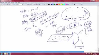
- GaN-on-Diamond Substrates: This technology showcases superior thermal management capabilities beneficial for high-power RF applications. The combination of GaN's properties with Diamond's exceptional thermal conductivity presents opportunities for more efficient and reliable devices.
- Selective Area Growth (SAG): SAG allows for the growth of compound semiconductors in specific, defined regions, which is particularly useful in Photonic Integrated Circuits (PICs). This targeted growth aids in minimizing material waste and enhances component performance by ensuring uniformity and reducing defects.
- Epitaxial Lift-Off (ELO): ELO is a transformation technique that permits the transfer of thin layers of compound semiconductors to flexible or reusable substrates. This innovation is particularly valuable for developing lightweight and flexible electronic devices.
These innovations collectively signify not just advancements in material science but also enable the diversification of applications in sectors like telecommunications, quantum computing, and autonomous systems. With these techniques, the integration of high-performance devices becomes more feasible, thus accelerating the deployment of next-generation technologies.
Youtube Videos
Audio Book
Dive deep into the subject with an immersive audiobook experience.
GaN-on-Diamond
Chapter 1 of 4
🔒 Unlock Audio Chapter
Sign up and enroll to access the full audio experience
Chapter Content
GaN-on-Diamond Superior thermal management for high-power RF Substrates
Detailed Explanation
GaN-on-Diamond refers to the technique of using gallium nitride (GaN) material on a diamond substrate to create devices that have better thermal management. This means that they can handle heat more effectively, which is crucial for high-power applications like radio frequency (RF) systems. When devices generate power, they also produce heat. Using diamond, which has excellent thermal conductivity, helps dissipate this heat efficiently, resulting in more reliable and efficient devices.
Examples & Analogies
Think of a computer processor that gets hot when it's working hard. If it's sitting on a regular surface, it might overheat. But if you place it on a very good heat sink (like diamond in this case), it cools down much better. This is similar to what GaN-on-Diamond does for RF devices.
Selective Area Growth (SAG)
Chapter 2 of 4
🔒 Unlock Audio Chapter
Sign up and enroll to access the full audio experience
Chapter Content
Selective Area Growth Growth of compound semiconductors only in defined zones for (SAG) PICs
Detailed Explanation
Selective Area Growth (SAG) is a fabrication technique that allows for the growth of semiconductor materials in specific sections of a substrate. This means that rather than coating the entire surface with a semiconductor material, growth occurs only in designated areas. This is especially useful for photonic integrated circuits (PICs), where different parts of the circuit can have different materials optimized for their specific functions, leading to better performance and efficiency.
Examples & Analogies
It's like painting a canvas where you only want certain colors in specific sections. Instead of painting the whole canvas, you use stencils to apply paint only where needed, making sure that each area has the right color to achieve the desired design.
Wafer Bonding
Chapter 3 of 4
🔒 Unlock Audio Chapter
Sign up and enroll to access the full audio experience
Chapter Content
Wafer Bonding Bonding III-V materials to silicon photonics platforms
Detailed Explanation
Wafer Bonding is a process where different types of semiconductor materials, particularly III-V semiconductors (like gallium arsenide), are bonded to silicon substrates. This integration is significant because silicon is already widely used in electronic devices. By combining III-V materials with silicon, manufacturers can create devices that leverage the unique advantages of both materials, such as enhanced light emission and better electronic properties, which are crucial for photonic devices.
Examples & Analogies
Think about making a sandwich. The bread is the silicon base, while the toppings (lettuce, tomato, etc.) are the III-V materials that add flavor and texture. By combining these layers, you create a much more enjoyable and functional meal than if you had just plain bread or just toppings alone.
Epitaxial Lift-Off (ELO)
Chapter 4 of 4
🔒 Unlock Audio Chapter
Sign up and enroll to access the full audio experience
Chapter Content
Epitaxial Lift-Off (ELO) Allows transfer of thin compound layers to flexible or reusable substrates
Detailed Explanation
Epitaxial Lift-Off (ELO) is a technique that enables the transfer of thin layers of compound semiconductor materials to different types of substrates, including flexible ones. This is particularly important for applications that require lightweight and bendable devices. By transferring only thin layers, it also reduces material waste and can lower costs. This technique is instrumental in developing flexible electronic devices that can be used in new applications like wearable technology.
Examples & Analogies
Imagine peeling an apple. When you peel off the skin, you're left with just the thin layer. ELO works similarly, where it removes a thin layer of semiconductor while leaving the bulk material behind, allowing you to place that thin layer onto a different surface which can adapt to various shapes and uses.
Key Concepts
-
GaN-on-Diamond Substrates: Enhance thermal management in high-power RF devices.
-
Selective Area Growth (SAG): Optimizes material usage by allowing growth in defined areas.
-
Epitaxial Lift-Off (ELO): Facilitates the transfer of semiconductor layers to flexible substrates.
Examples & Applications
GaN-on-Diamond substrates are used in advanced radar systems and high-efficiency telecommunications.
Selective Area Growth techniques are used in Photonic Integrated Circuits to improve yield and performance.
Epitaxial Lift-Off is critical in developing flexible displays and wearable sensors.
Memory Aids
Interactive tools to help you remember key concepts
Rhymes
GaN in the heat, with Diamond to greet, thermal management can't be beat!
Stories
Imagine a semiconductor factory where GaN meets Diamond, becoming the king of thermal management. With SAG, they build only where needed, saving room and costs, while ELO helps create devices that twist and turn, just like our favorite toys.
Memory Tools
Remember 'GSE' for GaN, SAG, and ELO – the three pillars of the latest innovations in semiconductor fabrication!
Acronyms
SAG = Strategic Area Growth!
Flash Cards
Glossary
- GaNonDiamond Substrates
A technology that combines Gallium Nitride (GaN) with Diamond for improved thermal management in high-power RF applications.
- Selective Area Growth (SAG)
A technique that allows the selective growth of semiconductors in predefined areas, optimizing material usage and component quality.
- Epitaxial LiftOff (ELO)
A method that facilitates the transfer of thin layers of semiconductor materials to flexible substrates, enabling innovative electronics.
Reference links
Supplementary resources to enhance your learning experience.