
Key Emerging Materials and Trends
Interactive Audio Lesson
Listen to a student-teacher conversation explaining the topic in a relatable way.
Wide Bandgap and Ultra-Wide Bandgap Semiconductors
🔒 Unlock Audio Lesson
Sign up and enroll to listen to this audio lesson

Today, we're going to explore **Wide Bandgap** (WBG) and **Ultra-Wide Bandgap** (UWBG) semiconductors. Can anyone tell me what they think these terms mean?

Do they refer to semiconductors that can operate at higher voltages and temperatures?
Exactly! WBG and UWBG materials like GaN and SiC can withstand higher voltages and frequencies than silicon. They are crucial for RF and power electronics. Remember, WBG allows for higher efficiency!

What about their applications in real life?
Great question! These materials are used in renewable energy systems, electric vehicles, and telecommunications—essential for 5G. Think 'WBG = Power & Efficiency'!
Nanostructured Compound Semiconductors
🔒 Unlock Audio Lesson
Sign up and enroll to listen to this audio lesson

Now let's shift to **2D and nanostructured semiconductors**. What do you know about materials like MoS₂ or GaSe?

Aren't they super thin and flexible?
Exactly! Their atomic-scale thickness leads to quantum confinement effects. We see applications in flexible displays and wearable sensors. Remember the acronym 'FQW'—Flexible, Quantum, Wearable!

Can they be integrated into existing systems?
Yes, they can integrate well into electronic devices, making them flexible and adaptable.
Heterogeneous Integration with Silicon
🔒 Unlock Audio Lesson
Sign up and enroll to listen to this audio lesson
Heterogeneous integration is an essential trend. How do you think it combines different semiconductor technologies?
By combining high-speed logic with RF technologies?
Right! This allows for simultaneous integration of photonics and silicon devices on a single chip. Platforms like GaN-on-Silicon are key here. Remember 'Heres the Integration = Heterogeneous Integration'!
What advantages does that have?
It leads to compact design and improved performance, critical for applications such as 5G technology.
Introduction & Overview
Read summaries of the section's main ideas at different levels of detail.
Quick Overview
Standard
This section discusses crucial emerging materials like wide bandgap (WBG) and ultra-wide bandgap (UWBG) semiconductors, highlighting their applications and advantages. It also covers nanostructured semiconductors and heterogeneous integration with silicon, emphasizing their roles in advancing electronics and photonics.
Detailed
Emerging Materials in Compound Semiconductors
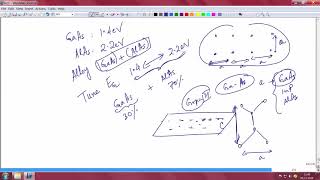
This section focuses on significant advancements in the field of compound semiconductors, particularly emphasizing Wide Bandgap (WBG) and Ultra-Wide Bandgap (UWBG) semiconductors. WBG materials, such as Gallium Nitride (GaN), Silicon Carbide (SiC), Diamond, Gallium Oxide (Ga₂O₃), and Aluminum Nitride (AlN), offer enhanced operational capabilities, including higher voltage, frequency, and temperature tolerances compared to traditional semiconductors like silicon. The applications of these materials span across RF (radio frequency) and power electronics, renewable energy solutions, and fast-charging technologies, making electronic devices smaller, more efficient, and reliable.
Nanostructured Semiconductors
2D and nanostructured compound semiconductors, including materials such as Indium Selenide (InSe), Gallium Selenide (GaSe), and Molybdenum Disulfide (MoS₂), exhibit unique advantages due to their atomic-scale thickness. This allows for quantum confinement, leading to applications in flexible electronics, neuromorphic computing, and wearable sensors. The section illustrates how these innovative materials are paving the way for future electronic and photonic devices.
Heterogeneous Integration
Another significant trend highlighted in this section is the heterogeneous integration of compound semiconductors with silicon (CMOS). This integration combines logic with high-speed opposers, facilitating the monolithic integration of photonics, RF, and logic on the same chip. Platforms such as GaN-on-Silicon, InP-on-Silicon, and GaAs-on-SOI are pivotal in these advancements. The overall impact of these key trends reaffirms compound semiconductors as fundamental to realizing advancements in electronics, particularly in future applications in 5G technology and smart energy systems.
Youtube Videos
Audio Book
Dive deep into the subject with an immersive audiobook experience.
Wide Bandgap (WBG) and Ultra-Wide Bandgap (UWBG) Semiconductors
Chapter 1 of 3
🔒 Unlock Audio Chapter
Sign up and enroll to access the full audio experience
Chapter Content
Wide Bandgap (WBG) and Ultra-Wide Bandgap (UWBG) Semiconductors
| Material | Bandgap (eV) | Applications |
|---|---|---|
| GaN | ~3.4 | RF, power electronics, 5G |
| SiC | ~3.3 | EV inverters, power conversion |
| Diamond | ~5.5 | High-power electronics (R&D) |
| Ga₂O₃ | ~4.8 | Low-cost high-voltage switches |
| AlN | ~6.2 | Deep UV LEDs, RF components |
- Enable higher voltage, frequency, and temperature operation than traditional semiconductors.
- Lead to smaller, more efficient, and more reliable power and RF devices.
Detailed Explanation
Wide Bandgap (WBG) and Ultra-Wide Bandgap (UWBG) semiconductors are materials that have a larger energy gap (bandgap) compared to traditional materials like silicon. The bandgap is measured in electronvolts (eV), where a larger bandgap allows these materials to operate at higher voltages, frequencies, and temperatures. For instance, materials like Gallium Nitride (GaN) and Silicon Carbide (SiC) have bandgaps around 3.4 eV and 3.3 eV, respectively, making them suitable for high-power and radio-frequency applications. These semiconductors also contribute to the development of smaller, more efficient devices, meaning they can manage energy better and are more reliable compared to older technologies, ideal for growing industries like 5G technology.
Examples & Analogies
Think of WBG and UWBG semiconductors like high-performance sports cars that can handle higher speeds and tighter turns compared to regular cars. Just as a sports car offers enhanced capabilities, these semiconductors provide better performance in demanding electronic applications, allowing for faster data transmission in 5G networks.
2D and Nanostructured Compound Semiconductors
Chapter 2 of 3
🔒 Unlock Audio Chapter
Sign up and enroll to access the full audio experience
Chapter Content
2D and Nanostructured Compound Semiconductors
- Examples: InSe, GaSe, MoS₂-based heterostructures
- Advantages:
- Atomic-scale thickness → quantum confinement
- Flexible, transparent electronics
- Applications: Wearable sensors, neuromorphic computing, flexible displays.
Detailed Explanation
2D and nanostructured semiconductors are materials that are extremely thin, often just a few atoms thick. This atomic-scale thickness allows them to exhibit unique properties due to quantum confinement, where the behavior of particles is different from what is observed in bulk materials. These semiconductors are not only flexible and transparent, making them excellent for innovative electronic applications, but they can also be used in cutting-edge areas like wearable sensors and neuromorphic computing systems, which mimic human brain functions. This rapid advancement showcases how materials engineered at the nanoscale are paving the way for next-generation electronics.
Examples & Analogies
Imagine a piece of paper that is folded into a small origami figure. The thinness of the paper allows it to take on unique shapes and functions. Similarly, 2D semiconductors, with their thin structure, can transform how electronics work and enable features like flexible displays on wearable tech, much like how the origami figure can fit into various shapes.
Heterogeneous Integration with Silicon
Chapter 3 of 3
🔒 Unlock Audio Chapter
Sign up and enroll to access the full audio experience
Chapter Content
Heterogeneous Integration with Silicon
- Combines CMOS (logic) with III-V semiconductors (high-speed/optoelectronics)
- Enables monolithic integration of photonics, RF, and logic on the same chip
- Platforms: GaN-on-Si, InP-on-Si, GaAs-on-SOI.
Detailed Explanation
Heterogeneous integration is a technology that allows different types of semiconductor materials to be combined on a single chip. By integrating traditional complementary metal-oxide-semiconductor (CMOS) technology, which is used for digital logic, with III-V semiconductors known for their high-speed and optoelectronic properties, we can create chips that are more powerful and versatile. This integration allows various functions, like photonics (light-based technologies) and radio frequency components, to coexist on the same physical structure, leading to more compact devices that can handle multiple tasks simultaneously.
Examples & Analogies
Think of heterogeneous integration like a multi-functional kitchen appliance that combines a blender, a food processor, and a juicer. Instead of having separate devices for each task taking up space, this single appliance can perform all functions efficiently and save time—just as chips that integrate different semiconductor technologies provide improved capabilities and space efficiency in electronic devices.
Key Concepts
-
WBG Semiconductors: These materials, including GaN and SiC, provide enhanced performance in high-voltage and high-frequency applications.
-
Nanostructured Semiconductors: 2D materials like MoS₂ and InSe have unique electronic properties due to their atomic thickness, enabling flexible applications.
-
Heterogeneous Integration: This combines different semiconductor types to enhance performance and functionality in electronic devices.
Examples & Applications
GaN is widely used in RF applications for 5G systems due to its high efficiency and thermal performance.
MoS₂ enables flexible electronic sensors that can be incorporated into wearable health-monitoring devices.
Memory Aids
Interactive tools to help you remember key concepts
Rhymes
WBGs ready to power, / In devices they hold the power / SiC and GaN take the stage, / Flexibility in every age.
Stories
Imagine a transformer made of GaN, it powers a charger, allowing devices to run at super speeds. Every device keeps getting smaller and efficient, thanks to WBG semiconductors paving the way.
Memory Tools
FLEC: Flexible, Low-cost, Efficient, Compact - Key attributes of 2D materials and their applications.
Acronyms
HIC
Heterogeneous Integration Chip - Represents the combination of CMOS with compound semiconductors.
Flash Cards
Glossary
- Wide Bandgap (WBG) Semiconductors
Semiconductors that have a wider bandgap than silicon, allowing for higher voltages and temperatures in applications.
- UltraWide Bandgap (UWBG) Semiconductors
Semiconductors with an even wider bandgap than WBG materials, enabling extreme applications like high-power electronics and specialized optics.
- Quantum Confinement
The phenomenon where quantum effects dominate the properties of materials due to their reduced dimensions, typical in 2D materials.
- Heterogeneous Integration
Combining different types of semiconductors, typically compound semiconductors with silicon, to improve performance and reduce size in electronics.
Reference links
Supplementary resources to enhance your learning experience.