
Energy Band Diagrams
Enroll to start learning
You’ve not yet enrolled in this course. Please enroll for free to listen to audio lessons, classroom podcasts and take practice test.
Interactive Audio Lesson
Listen to a student-teacher conversation explaining the topic in a relatable way.
Introduction to Energy Band Diagrams
🔒 Unlock Audio Lesson
Sign up and enroll to listen to this audio lesson

Today, we're discussing energy band diagrams. Can anyone tell me why these diagrams are important in semiconductor physics?

Are they used to show how electrons behave in different materials?
Exactly! These diagrams help us visualize the energy levels available to electrons. For intrinsic semiconductors, the Fermi level is right in the middle. Why do you think that matters?

It helps in determining the conductivity of the material, right?
Correct! And when we introduce impurities into the materials, like in n-type and p-type semiconductors, how does that affect the Fermi level?

The Fermi level moves closer to the conduction band for n-type and to the valence band for p-type?
Exactly! So, the position of the Fermi level shapes how we understand electron and hole concentrations in semiconductors.
In summary, energy band diagrams are vital for predicting how semiconductors will behave under different conditions, impacting their use in electronics.
Fermi Level in n-Type and p-Type Semiconductors
🔒 Unlock Audio Lesson
Sign up and enroll to listen to this audio lesson

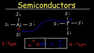
Now, let’s delve into n-type semiconductors. Who can explain what occurs when phosphorus is added to silicon?

Phosphorus has five valence electrons, and when it's added, it creates extra electrons, making the material conductive.
Great! And where does the Fermi level shift in this scenario?
It moves closer to the conduction band!
Precisely! Now, who can discuss the p-type semiconductors and the effect of adding boron?
Boron has only three valence electrons, so it creates holes, and the Fermi level moves closer to the valence band.
Exactly! The introduction of these impurities significantly alters the electronic properties and conductivity of the semiconductor. To wrap up, understanding where the Fermi level sits helps us evaluate the semiconductor's behavior in devices.
Introduction & Overview
Read summaries of the section's main ideas at different levels of detail.
Quick Overview
Standard
This section discusses energy band diagrams for intrinsic, n-type, and p-type semiconductors, explaining the significance of the Fermi level in determining the conductivity and electron energy states within different semiconductor materials.
Detailed
Energy Band Diagrams
Energy band diagrams are a vital tool for visualizing and understanding the electronic properties of semiconductors. These diagrams depict the various energy levels available to electrons in a material and illustrate the differences in behavior between intrinsic semiconductors, n-type semiconductors, and p-type semiconductors.
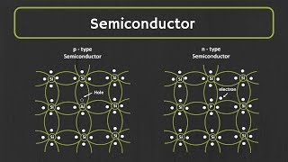
- Intrinsic Semiconductors: The energy band diagram for intrinsic semiconductors, such as pure silicon, has the Fermi level positioned in the middle of the energy gap between the valence band and the conduction band.
- n-Type Semiconductors: For n-type semiconductors, where donor impurities are introduced (for example, phosphorus in silicon), the Fermi level shifts closer to the conduction band. This shift indicates a higher concentration of electrons, which increases conductivity.
- p-Type Semiconductors: Conversely, in p-type semiconductors, acceptor impurities (such as boron) are introduced, causing the Fermi level to move closer to the valence band. This results in a predominance of holes, which act as positive charge carriers, impacting the material's conductivity.
Understanding these diagrams is significant for analyzing how semiconductors function in various applications, including diodes and transistors.
Youtube Videos


Audio Book
Dive deep into the subject with an immersive audiobook experience.
Purpose of Energy Band Diagrams
Chapter 1 of 4
🔒 Unlock Audio Chapter
Sign up and enroll to access the full audio experience
Chapter Content
● Visualize energy levels:
Detailed Explanation
Energy band diagrams serve as a visual tool to understand the distribution of energy levels in semiconductor materials. They help illustrate the positions of important energy levels, such as the valence band, conduction band, and the Fermi level in different types of semiconductors.
Examples & Analogies
Think of an energy band diagram like a mountain range. The peaks are the energy levels in the material, and the valleys represent the bands where electrons can reside. Just as climbers prefer to stay at higher altitudes, electrons naturally occupy higher energy states in the conduction band.
Energy Band Diagram for Intrinsic Semiconductors
Chapter 2 of 4
🔒 Unlock Audio Chapter
Sign up and enroll to access the full audio experience
Chapter Content
○ Intrinsic: Fermi level in the middle.
Detailed Explanation
In intrinsic semiconductors, which are pure and undoped, the Fermi level—the energy level at which the probability of finding an electron is 50%—is positioned in the middle of the energy gap between the valence band and the conduction band. This reflects a balance between available energy states for electrons and holes, indicating that both can be generated equally at thermal equilibrium.
Examples & Analogies
Imagine a balanced seesaw. When both sides have equal weight, the seesaw remains level. Similarly, in intrinsic semiconductors, the equal distribution of energy levels for electrons and holes keeps the Fermi level centered.
Energy Band Diagram for n-type Semiconductors
Chapter 3 of 4
🔒 Unlock Audio Chapter
Sign up and enroll to access the full audio experience
Chapter Content
○ n-type: Fermi level closer to conduction band.
Detailed Explanation
In n-type semiconductors, which are doped with donor impurities (like phosphorus), there are more electrons than holes. Consequently, the Fermi level shifts closer to the conduction band, reflecting the higher energy states available for conduction. The increased number of electrons makes it easier for electrical current to flow through the material.
Examples & Analogies
Consider a crowded elevator. If several people (electrons) are waiting at a particular floor (the conduction band), the likelihood of the elevator being filled with people increases, making it easier to enter the elevator. Similarly, in an n-type semiconductor, the increased electron population enables better conductivity.
Energy Band Diagram for p-type Semiconductors
Chapter 4 of 4
🔒 Unlock Audio Chapter
Sign up and enroll to access the full audio experience
Chapter Content
○ p-type: Fermi level closer to valence band.
Detailed Explanation
In p-type semiconductors, which are doped with acceptor impurities (like boron), there are more holes available for conduction. The Fermi level thus shifts closer to the valence band, indicating a surplus of holes that facilitate current flow. This characteristic defines how p-type materials conduct electricity mainly through the movement of holes rather than electrons.
Examples & Analogies
Imagine a group of friends trying to find seating in a cafe. If more people have left (creating holes), there are more available seats for new customers (holes for electrons to occupy). Similarly, p-type semiconductors are easier to conduct when there are many holes available.
Key Concepts
-
Energy Band Diagram: A representation of energy levels in semiconductor materials.
-
Fermi Level: The energy level that indicates the distribution of electrons.
-
n-Type vs p-Type: The difference in conductivity based on added impurities.
-
Intrinsic Behavior: How pure semiconductors behave without doping.
Examples & Applications
In an intrinsic semiconductor, the Fermi level is centered, indicating equal potential for electrons and holes.
In an n-type semiconductor, the addition of phosphorus shifts the Fermi level toward the conduction band, reflecting higher electron concentration.
In a p-type semiconductor, the introduction of boron moves the Fermi level closer to the valence band, indicating a predominance of holes.
Memory Aids
Interactive tools to help you remember key concepts
Rhymes
Fermi's middle, semiconductors too, n-type goes up, p-type goes blue.
Stories
Once in a semiconductor town, Fermi lived in the middle, but when donors came around, he shifted up, and holes made him brittle.
Memory Tools
Fermi's Fantastic Move - FM: n-type moves Fermi to the conduction side, p-type moves it to valence for a ride.
Acronyms
DEEP
Donor Electrons Enrich
P-type empties for holes.
Flash Cards
Glossary
- Energy Band Diagram
A graphical representation of the energy levels in a material, showing the valence and conduction bands.
- Fermi Level
The energy level at which the probability of finding an electron is 50%, indicating the distribution of electrons in energy bands.
- Intrinsic Semiconductor
A pure semiconductor without any significant dopants that affect its electrical characteristics.
- nType Semiconductor
A semiconductor that is doped with elements that have extra valence electrons, increasing the number of free electrons.
- pType Semiconductor
A semiconductor that is doped with elements that have fewer valence electrons, creating holes as charge carriers.
Reference links
Supplementary resources to enhance your learning experience.