
Mass Action Law
Enroll to start learning
You’ve not yet enrolled in this course. Please enroll for free to listen to audio lessons, classroom podcasts and take practice test.
Interactive Audio Lesson
Listen to a student-teacher conversation explaining the topic in a relatable way.
Introduction to the Mass Action Law
🔒 Unlock Audio Lesson
Sign up and enroll to listen to this audio lesson

Today, we're going to discuss an important concept in semiconductor physics known as the Mass Action Law. Can anyone tell me what this law describes?

Does it have something to do with electrons and holes in semiconductors?
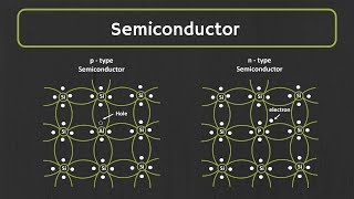
Exactly! The Mass Action Law states that in an intrinsic semiconductor, the product of the concentrations of electrons, n, and holes, p, equals the square of the intrinsic carrier concentration, ni. So, we have the equation ni² = n · p.

So, if we know how many electrons are present, we can find out how many holes there are, right?
That's correct! And this relationship helps us understand how the semiconductor behaves, especially as conditions change. For instance, what happens to electron and hole concentrations if we raise the temperature?

Wouldn’t they both increase?
Yes, as temperature rises, more electrons can jump to the conduction band, leading to more electron-hole pairs. Great understanding!

Can you summarize the Mass Action Law again?
Of course! The Mass Action Law states that ni² = n · p, which means the concentrations of electrons and holes are linked by the intrinsic carrier concentration. If either increases or decreases, the other must adjust to maintain the product. This principle is fundamental for interpreting semiconductor behavior.
Implications of the Mass Action Law
🔒 Unlock Audio Lesson
Sign up and enroll to listen to this audio lesson

Let's talk about the implications of the Mass Action Law in practical scenarios. How do you think this law helps in the design of semiconductor devices?
It should help engineers know how many charge carriers they need for a device to work properly.
Exactly! By knowing the relationship defined by the Mass Action Law, engineers can optimize the doping levels of semiconductors to achieve desired electrical properties. Can you think of an example where this law is applied?
In solar cells? They rely on semiconductors, right?
Yes! Solar cells use semiconductors, and understanding their electron and hole concentrations is crucial for maximizing their efficiency. Temperature variations can significantly affect performance, and the Mass Action Law aids in predicting these changes.
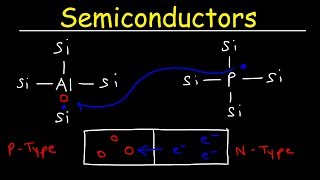
And if we use a different doping element, won’t that change the carrier concentrations?
Exactly! Different dopants can lead to either an increase in electron or hole concentration, depending on whether it's an n-type or p-type semiconductor.
Summarize the importance of the Mass Action Law in engineering?
Sure! The Mass Action Law is vital for designing semiconductor devices by predicting how changes in temperature and carrier concentrations affect overall performance.
Introduction & Overview
Read summaries of the section's main ideas at different levels of detail.
Quick Overview
Standard
The Mass Action Law illustrates the relationship between the concentration of charge carriers in an intrinsic semiconductor. Specifically, it describes how the concentration of electrons (n) and holes (p) relates to the intrinsic carrier concentration (ni), encapsulated in the equation ni² = n · p. This principle is critical for understanding how semiconductors function under different conditions.
Detailed
Mass Action Law
The Mass Action Law is a fundamental principle in semiconductor physics, particularly relevant for understanding intrinsic semiconductors. According to this law, in an intrinsic semiconductor, the product of the concentration of electrons (n) and holes (p) is constant and equal to the square of the intrinsic carrier concentration (
^2 = ni2). This relationship can be expressed as:
ni² = n · p
where:
- n: concentration of electrons
- p: concentration of holes
- ni: intrinsic carrier concentration
Significance of the Mass Action Law
This law is significant because it helps predict the behavior of semiconductors under various conditions, especially when dealing with temperature changes or the introduction of impurities (doping). Understanding this principle is pivotal for designing and analyzing semiconductor devices such as diodes and transistors.
Youtube Videos


Audio Book
Dive deep into the subject with an immersive audiobook experience.
Understanding the Mass Action Law
Chapter 1 of 2
🔒 Unlock Audio Chapter
Sign up and enroll to access the full audio experience
Chapter Content
In an intrinsic semiconductor:
ni² = n ⋅ p
Detailed Explanation
The Mass Action Law states that, in an intrinsic semiconductor, the intrinsic carrier concentration squared (ni²) is equal to the product of the concentration of electrons (n) and the concentration of holes (p). This relationship demonstrates a pivotal concept in semiconductor physics, indicating that the number of electrons and holes in an intrinsic semiconductor are inherently linked through this equation. As the number of electrons increases, the number of holes will decrease, and vice versa, maintaining the equality of ni².
Examples & Analogies
Think of a busy train station where passengers represent electrons and the empty seats represent holes. If more passengers (electrons) arrive, some will need to sit down, filling up the empty seats (holes). The total effect maintains a balance, illustrating how the Mass Action Law works—an increase in one (electrons) decreases the other (holes), keeping a constant ratio according to the intrinsic carrier concentration.
Components of the Equation
Chapter 2 of 2
🔒 Unlock Audio Chapter
Sign up and enroll to access the full audio experience
Chapter Content
Where:
● n: concentration of electrons
● p: concentration of holes
● ni: intrinsic carrier concentration
Detailed Explanation
In the Mass Action Law equation, we have three crucial components: n, p, and ni. The variable 'n' represents the concentration of electrons in the semiconductor, while 'p' signifies the concentration of holes. 'ni', or the intrinsic carrier concentration, is a constant for each material, representing the number of charge carriers present in a pure semiconductor without any dopants. This distinction is essential for understanding how semiconductors behave, especially under different conditions such as temperature or doping.
Examples & Analogies
Imagine a classroom where students can either sit at desks (electrons) or stand in the aisles (holes). The number of students (carriers) is fixed by the classroom size (intrinsic carrier concentration). If more students choose to sit at desks (electrons), fewer must stand (holes). This illustrates how the balance of carriers works in semiconductors, just like in the classroom scenario.
Key Concepts
-
Mass Action Law: Defines the relationship between electron and hole concentrations in intrinsic semiconductors.
-
Intrinsic Carrier Concentration (ni): The equilibrium concentration of charge carriers in a pure semiconductor.
-
Charge Carriers: Electrons and holes that participate in electrical conduction.
Examples & Applications
In an intrinsic semiconductor at room temperature, if the intrinsic carrier concentration ni is 1.5 × 10^10 cm^-3, then the product of the electron and hole concentrations n and p must be (1.5 × 10^10)^2 = 2.25 × 10^20 cm^-6.
If the electron concentration n is found to be 1 × 10^10 cm^-3, then the hole concentration p can be calculated as p = ni²/n = 2.25 × 10^20 / (1 × 10^10) = 2.25 × 10^10 cm^-3.
Memory Aids
Interactive tools to help you remember key concepts
Rhymes
In a semiconductor, where electrons play, holes are there to balance the way.
Stories
Imagine a balanced see-saw: on one side, electrons sit, on the other, holes fit. Together, they are equal, it’s the law!
Memory Tools
Remember: Nifty Intrinsic Carriers (ni) = Next (n) and Pals (p) together!
Acronyms
MAL
Mass Action Law - Remember it helps you see how n and p relate.
Flash Cards
Glossary
- Intrinsic Carrier Concentration (ni)
The number of electrons and holes generated in a pure semiconductor at thermal equilibrium.
- Electrons (n)
Negatively charged particles that conduct electricity in semiconductors.
- Holes (p)
Positively charged vacancies in a semiconductor that facilitate charge conduction.
Reference links
Supplementary resources to enhance your learning experience.