
Introduction to Semiconductor Physics
Enroll to start learning
You’ve not yet enrolled in this course. Please enroll for free to listen to audio lessons, classroom podcasts and take practice test.
Interactive Audio Lesson
Listen to a student-teacher conversation explaining the topic in a relatable way.
Overview of Semiconductor Physics
🔒 Unlock Audio Lesson
Sign up and enroll to listen to this audio lesson

Welcome, everyone! Today, we’ll delve into semiconductor physics, which is essential for understanding modern electronics. Can anyone tell me what a semiconductor is?

Isn't it a material that conducts electricity, but not as well as metals?
Exactly! Semiconductors have electrical conductivity lying between conductors and insulators. For example, silicon and germanium are commonly used semiconductors. Let's remember this with the acronym **S**ilicon and **G**ermanium – **'SG' for Semiconductors' Goodness**!

What about their behavior?
Great question! Semiconductors behave based on energy band theory, which involves three main components: the valence band, conduction band, and forbidden energy gap. Can someone explain what the forbidden energy gap means?

It's the energy range where no electron states can exist, right?
Exactly! This gap is crucial because it determines the conductivity of a semiconductor, which we'll explore further.
Classification of Materials by Conductivity
🔒 Unlock Audio Lesson
Sign up and enroll to listen to this audio lesson

Now let’s classify materials based on conductivity. What classification can we think of?

I know there are conductors, semiconductors, and insulators!
Correct! Let’s break down their characteristics. Conductors like copper have very high conductivity due to overlapping energy bands. Can anyone tell me what semiconductors and insulators look like?
Semiconductors have a moderate conductivity, about 1 eV for the energy gap, and insulators have very low conductivity with energy gaps greater than 5 eV!
Well done! Remember, for semiconductors, we often remember **1.0 eV** as a critical threshold for understanding.
Intrinsic and Extrinsic Semiconductors
🔒 Unlock Audio Lesson
Sign up and enroll to listen to this audio lesson
Let’s discuss intrinsic semiconductors first. What do you think they are?
Aren't they pure materials without impurities?
That's right! At absolute zero, they behave like insulators, but as temperature increases, electron-hole pairs can form. How does this change with extrinsic semiconductors?
They are doped with impurities to modify their conductivity!
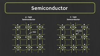
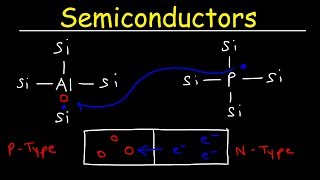
Exactly! We can categorize them into n-type, where electrons are the majority carriers, and p-type, where holes are predominant. Remember the acronym **N**egative for n-type and **P**ositive for p-type to help memorize this!
Energy Band Diagrams
🔒 Unlock Audio Lesson
Sign up and enroll to listen to this audio lesson
Next, let’s explore energy band diagrams! Why do you think they are important?
They show us how energy levels are arranged in semiconductors!
Absolutely! They help us visualize the Fermi level's position in intrinsic, n-type, and p-type semiconductors. Why might the Fermi level differ among these?
Because in n-type, it’s closer to the conduction band, and in p-type, it’s closer to the valence band!
Well articulated! This difference is crucial for understanding how semiconductors manage charge carriers.
Drift and Diffusion Currents
🔒 Unlock Audio Lesson
Sign up and enroll to listen to this audio lesson
Finally, we should discuss current mechanisms. Who can explain drift current?
Is it the current caused by an electric field applied on charge carriers?
Exactly! The equation for drift current is I_drift = q n μ E. What about diffusion current?
That’s caused by the concentration gradient!
Spot on! The diffusion current equation is I_diffusion = q D (dn/dx). It's important we grasp both currents as they contribute to total current in semiconductors.
Introduction & Overview
Read summaries of the section's main ideas at different levels of detail.
Quick Overview
Standard
Semiconductor physics lays the groundwork for understanding how materials with intermediate conductivity behave. This section explores the classification of materials based on conductivity, atomic structure, intrinsic and extrinsic semiconductors, and current mechanisms, while also emphasizing their importance in modern electronics.
Detailed
Introduction to Semiconductor Physics
In the realm of electronics, semiconductors serve as the crucial link between conductors and insulators, laying the foundation for devices like diodes and transistors. This section presents an overview of semiconductor properties, including the energy band theory that describes their behavior through three primary bands: valence band, conduction band, and the forbidden energy gap (Eg).
Key Topics Covered:
- Classification of Materials:
- Semiconductors have moderate conductivity, typified by silicon and germanium, while conductors and insulators are characterized by high and very low conductivity, respectively.
- Atomic Structure:
- The atomic arrangement of semiconductors, with four valence electrons in Si and Ge, promotes the formation of covalent bonds in a crystalline lattice. At absolute zero, these materials act as insulators, becoming conductive with increasing temperature.
- Intrinsic Semiconductors:
- Pure semiconductors devoid of impurities, where thermal excitation leads to the generation of electron-hole pairs, thereby increasing charge carrier concentration.
- Extrinsic Semiconductors:
- The doping process introduces impurities to control conductivity, creating n-type and p-type semiconductors with distinct majority and minority carriers.
- Energy Band Diagrams:
- These diagrams visualize the energy levels within semiconductors, critical for understanding the Fermi level positioning in intrinsic, n-type, and p-type materials.
- Currents in Semiconductors:
- The section discusses drift and diffusion currents, essential mechanisms governing the flow of electricity within these materials.
- Mass Action Law:
- Illustrates the relationship between electron and hole concentrations in intrinsic semiconductors, vital for understanding their conductivity.
In summary, this section provides essential insights into semiconductor physics, key for advancing technology in diodes, transistors, and many other electronic applications.
Youtube Videos

Audio Book
Dive deep into the subject with an immersive audiobook experience.
What Are Semiconductors?
Chapter 1 of 3
🔒 Unlock Audio Chapter
Sign up and enroll to access the full audio experience
Chapter Content
Semiconductors are materials with electrical conductivity between that of conductors and insulators. They are the foundation of modern electronics, used in devices like diodes, transistors, and integrated circuits.
Detailed Explanation
Semiconductors are unique materials that fall between conductors (like metals, which easily conduct electricity) and insulators (like rubber, which do not conduct electricity at all). They can control electrical currents and are essential for creating electronic devices such as diodes, which allow electricity to flow in one direction, and transistors, which can amplify or switch electronic signals. This ability makes semiconductors crucial for building integrated circuits that are used in everything from smartphones to computers.
Examples & Analogies
Think of a semiconductor like a faucet. When the faucet is closed (like an insulator), water (or electricity) cannot flow. When you open it slightly (like a semiconductor), you can control the flow of water—just enough to water your plants without flooding them, similar to how semiconductors can control electric currents in devices.
Common Semiconductor Materials
Chapter 2 of 3
🔒 Unlock Audio Chapter
Sign up and enroll to access the full audio experience
Chapter Content
● Common semiconductors: Silicon (Si) and Germanium (Ge)
Detailed Explanation
Two of the most commonly used semiconductor materials in electronics are Silicon (Si) and Germanium (Ge). Silicon is the most widely used due to its abundance, excellent electrical properties, and ability to form complex structures necessary for integrated circuits. Germanium was used in earlier semiconductor devices, but it is less common today due to higher costs and performance limitations compared to silicon.
Examples & Analogies
Imagine Silicon being the bread and Butter of the electronic world. Just like how bread is essential for various sandwiches and meals, Silicon is fundamental in creating countless electronic devices, from smartphones to computers. Germanium, on the other hand, is like a gourmet ingredient: it can enhance flavors (or performance) but is used less frequently due to cost.
Energy Band Theory
Chapter 3 of 3
🔒 Unlock Audio Chapter
Sign up and enroll to access the full audio experience
Chapter Content
● Energy band theory explains their behavior using valence band, conduction band, and forbidden energy gap (Eg).
Detailed Explanation
Energy band theory is a model that describes how electrons behave in a solid material, particularly semiconductors. In this model, there are two main energy bands to consider: the valence band, where electrons are usually found, and the conduction band, where electrons can move freely to conduct electricity. The energy gap, or band gap (Eg), is the energy required for an electron to jump from the valence band to the conduction band. In semiconductors, this gap is moderate in size, allowing some electrons to leap with the right amount of energy, which is influenced by temperature and doping.
Examples & Analogies
You can think of the energy bands like a staircase. The valence band is the ground floor where people (electrons) comfortably stand. The conduction band is a higher floor where people can run around freely. The forbidden gap is like the steps; unless someone has enough energy (like a strong push), they cannot jump from the ground floor to the upper floor. In semiconductors, as temperature increases, more people gain the energy required to climb those steps and reach the upper floor.
Key Concepts
-
Energy Band Theory: Describes the electron energy levels and their arrangement in semiconductors.
-
Intrinsic vs. Extrinsic: Distinguishes between pure semiconductors and those modified by doping.
-
Drift and Diffusion Currents: Key mechanisms for understanding charge movement in semiconductors.
-
Mass Action Law: Fundamental principle relating electron and hole concentrations in intrinsic semiconductors.
Examples & Applications
Silicon (Si) is the most widely used semiconductor material in electronic devices such as transistors and solar cells.
Germanium (Ge) was one of the first semiconductors used in early electronics but is now less common compared to silicon.
Memory Aids
Interactive tools to help you remember key concepts
Rhymes
In semiconductors, energy flows and glows, between the bands, where the charge carriers go.
Stories
Imagine a city where electrons are the workers and holes are the vacant jobs. In a semiconductor, when the city heats up, more workers can move into jobs, increasing activity.
Memory Tools
Remember 'N' for n-type as 'Negative' and 'P' for p-type as 'Positive' to recall their charge carriers.
Acronyms
SG for **S**emiconductors - **G**oodness, emphasizing Silicon and Germanium's importance.
Flash Cards
Glossary
- Semiconductor
Materials with electrical conductivity between that of conductors and insulators, essential for modern electronics.
- Intrinsic Semiconductor
Pure semiconductors without impurities, characterized by thermal excitation of electron-hole pairs.
- Extrinsic Semiconductor
Doped semiconductors that have altered conductivity due to the introduction of impurities.
- Energy Band Gap (Eg)
The energy range between the valence band and conduction band; critical for determining electrical conductivity.
- Electronhole pair
Created when an electron moves from the valence band to the conduction band, leaving behind a positive hole.
- Fermi Level
The energy level at which the probability of finding an electron is 50%; its position varies in intrinsic and extrinsic semiconductors.
- Doping
The addition of impurities to semiconductors to alter their electrical properties.
- Drift Current
Electric current caused by charge carriers moving in response to an applied electric field.
- Diffusion Current
Electric current resulting from the movement of charge carriers from high to low concentration areas.
- Mass Action Law
A principle that relates the concentration of electrons and holes in intrinsic semiconductors.
Reference links
Supplementary resources to enhance your learning experience.