
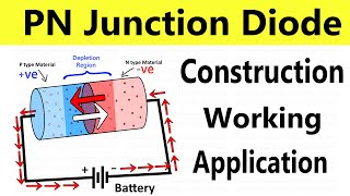
Formation of Depletion Region
Enroll to start learning
You’ve not yet enrolled in this course. Please enroll for free to listen to audio lessons, classroom podcasts and take practice test.
Interactive Audio Lesson
Listen to a student-teacher conversation explaining the topic in a relatable way.
Charge Carrier Diffusion
🔒 Unlock Audio Lesson
Sign up and enroll to listen to this audio lesson

Let's begin with the diffusion of charge carriers. When we join a p-type semiconductor with an n-type semiconductor, what happens to the electrons and holes?

I think electrons move from the n-type to the p-type region, right?
Exactly! Electrons from the n-type region diffuse into the p-type region. What about the holes?

Holes move from the p-type region into the n-type region.
Right! This movement of charge carriers is essential for forming what we call the depletion region. Can anyone tell me what happens when they get closer?

Once they meet, they recombine, leaving behind charged ions.
Perfect! This recombination creates a zone without mobile charge carriers, which is known as the depletion region. Remember, D for Depletion, where no charges reside.
Formation and Characteristics of the Depletion Region
🔒 Unlock Audio Lesson
Sign up and enroll to listen to this audio lesson
It's the area around the junction where there are no charge carriers because they’ve recombined.

Great! And why is this region important for diodes?

Because it creates an electric field that affects the flow of current when we apply voltage.
That's right! This electric field results in a built-in potential (V₀) which opposes further diffusion of electrons and holes. Can anyone think of how this impacts a diode’s operation?
It controls whether the diode allows current to pass through or not!
Exactly! The depletion region is crucial in determining the diode's behavior based on applied voltage.
Built-in Potential and its Effects
🔒 Unlock Audio Lesson
Sign up and enroll to listen to this audio lesson
Let’s dive deeper into the built-in potential. What do we mean by this term in the context of a PN junction?
Is it the potential difference that forms because of the additional charges left behind in the depletion region?
Spot on! This potential difference is a result of the electric field set up in the depletion region. Why do you think this is significant?
It means that a certain amount of voltage is required to allow current to flow through the junction.
Exactly! It helps define how diodes can be either forward-biased or reverse-biased, influencing their conducting state. Always keep in mind: built-in potential is 'V₀' and helps us understand a diode’s operational limits.
Applications of the Depletion Region
🔒 Unlock Audio Lesson
Sign up and enroll to listen to this audio lesson
Lastly, let’s discuss the applications of the depletion region in real-world devices. What are some examples you can think of?
I know they are used in diodes, but how exactly does the depletion region help?
Excellent question! In diodes, the depletion region allows for rectification of current, which is essential for converting AC to DC. Can anyone think of another example?
What about Zener diodes? They take advantage of the depletion region for voltage regulation.
Exactly! The depletion region is also critical in Zener diodes, which operate in a reverse breakdown state. Remember, how the depletion region behaves influences many applications in electronics!
Introduction & Overview
Read summaries of the section's main ideas at different levels of detail.
Quick Overview
Standard
When p-type and n-type materials are connected, electrons from the n-type region move towards the p-type region, while holes move towards the n-type region. This diffusion leaves behind charged ions, forming a depletion region devoid of free charge carriers and establishing an electric field across the junction.
Detailed
Formation of Depletion Region
When a p-type semiconductor (with high hole concentration) and an n-type semiconductor (with high electron concentration) are brought into contact, a process occurs that leads to the formation of a depletion region. This section covers the following key points:
- Diffusion of Charge Carriers: Electrons from the n-type region diffuse into the p-type region, while holes from the p-type region diffuse into the n-type region.
- Formation of the Depletion Region: As electrons and holes recombine, they leave behind immobile ions, which creates a charge-free zone known as the depletion region.
- Development of Electric Field: The charge imbalance in the depletion region gives rise to an electric field that opposes further diffusion, establishing a built-in potential (V₀) across the junction. This section is vital in understanding how diodes function and the behavior of semiconductor devices.
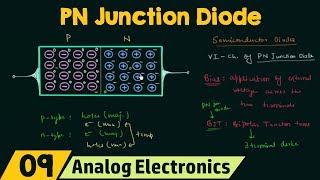
Youtube Videos

Audio Book
Dive deep into the subject with an immersive audiobook experience.
Diffusion of Charge Carriers
Chapter 1 of 3
🔒 Unlock Audio Chapter
Sign up and enroll to access the full audio experience
Chapter Content
● When p-type and n-type materials are joined, electrons diffuse from n to p, and holes diffuse from p to n.
Detailed Explanation
When a p-type semiconductor (which has an abundance of holes) is placed in contact with an n-type semiconductor (which has an abundance of electrons), a process called diffusion occurs. Electrons from the n-type region tend to move towards the p-type region, in search of holes to occupy. Similarly, holes from the p-type drift towards the n-type area. This movement occurs due to a concentration gradient, as charge carriers migrate from an area of high concentration to an area of low concentration.
Examples & Analogies
Think of an open door between two rooms filled with people; those in the more crowded room (the n-type) will move towards the less crowded room (the p-type) until the crowd levels out, representing the electrons moving to occupy holes.
Formation of Depletion Region
Chapter 2 of 3
🔒 Unlock Audio Chapter
Sign up and enroll to access the full audio experience
Chapter Content
● This movement leaves behind immobile ions, forming a depletion region (charge-free zone).
Detailed Explanation
As electrons move from the n-type region to the p-type region to fill the holes, they leave behind positively charged ion cores in the n-type material and negatively charged ion cores in the p-type material. These ion cores are unable to move, resulting in the creation of a region devoid of free charge carriers—known as the depletion region. This zone effectively becomes a barrier preventing additional current flow unless the junction is externally biased.
Examples & Analogies
Imagine a crowd dispersing from a park into two adjacent closed rooms. The empty space left behind signifies the depletion zone, where everyone has moved but no one is left to occupy that space.
Development of Electric Field
Chapter 3 of 3
🔒 Unlock Audio Chapter
Sign up and enroll to access the full audio experience
Chapter Content
● An electric field is developed across the junction, creating a built-in potential (V₀).
Detailed Explanation
The separation of charges created by the immobile positive and negative ions across the depletion region leads to the establishment of an electric field. This electric field resists further movement of charge carriers from the n-type to the p-type region. The potential energy associated with this electric field is known as the built-in potential (V₀), which plays a crucial role in the operation of the PN junction under different biasing conditions.
Examples & Analogies
Imagine building a hill in the middle of a flat road, which acts as a barrier. Just as cars struggle to go over the hill (the electric field), the built-in potential acts as a challenge for charge carriers to move across the PN junction without sufficient external energy to overcome it.
Key Concepts
-
Diffusion of charge carriers: The movement of electrons and holes across the PN junction.
-
Charge-free zone: The depletion region lacking free charge carriers due to recombination.
-
Built-in potential: The electric field established across the junction from charge imbalance.
Examples & Applications
In a silicon diode, when forward-biased, the depletion region decreases, allowing current to flow easily.
In a reverse-biased Zener diode, the depletion region widens, enabling voltage regulation under certain conditions.
Memory Aids
Interactive tools to help you remember key concepts
Rhymes
In junctions where p and n do meet, / The depletion forms, no charge to greet.
Stories
Imagine two friends, Electron and Hole, meet in a coffee shop. They find each other and combine to form a solid friendship, leaving their bags behind — this represents the depletion region!
Memory Tools
D E P L E T I O N: Diffusion Eliminates Positive and Negative, Leaving Everyone Tensions In Optically Neutralization.
Acronyms
V₀
'Voltage at Zero' meaning built-in potential that stops further carrier movement.
Flash Cards
Glossary
- Depletion Region
The area around the PN junction where charge carriers have recombined, leaving behind immobile ions and resulting in a charge-free zone.
- Builtin Potential (V₀)
The potential developed across the depletion region due to the electric field created by the charge imbalance.
- Charge Carriers
Electrons and holes that move within a semiconductor and are essential for current flow.
Reference links
Supplementary resources to enhance your learning experience.