
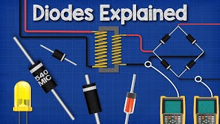
VI Characteristics of PN Junction Diode
Enroll to start learning
You’ve not yet enrolled in this course. Please enroll for free to listen to audio lessons, classroom podcasts and take practice test.
Interactive Audio Lesson
Listen to a student-teacher conversation explaining the topic in a relatable way.
Forward Bias Characteristics
🔒 Unlock Audio Lesson
Sign up and enroll to listen to this audio lesson

Today we are going to explore the VI characteristics of a PN junction diode, starting with forward bias. Can anyone tell me what happens when we connect a diode in forward bias?

The current should flow, right?
Exactly! Now, there is a threshold voltage, usually around 0.7 V for Silicon diodes. Can anyone guess what happens when we are below this voltage?

I think no current flows until we reach that threshold.
Correct! Once we surpass the threshold voltage, the current starts to increase exponentially. Remember this as the 'threshold ripple' for diodes when imagining current flow.

What causes the current to increase so rapidly after that point?
Great question! It’s due to the number of charge carriers being injected into the junction as we apply more voltage.

Can we see that in a graph?
Certainly! The graph shows how the current rises steeply once the threshold is crossed. Key point here: the diode conducts easily after reaching that threshold!
Reverse Bias Characteristics
🔒 Unlock Audio Lesson
Sign up and enroll to listen to this audio lesson

Now let's shift to reverse bias. Who can explain what happens when we apply reverse voltage to a PN junction diode?
I think the depletion region becomes wider, right?
Exactly! The depletion region does widen, and what's interesting is that the current remains very low, almost zero, until we hit the breakdown voltage. This is often referred to as 'reverse leakage current.'
What does 'breakdown voltage' mean?
The breakdown voltage is a critical point where, if the reverse voltage exceeds this value, the diode allows a large amount of current to flow. It’s important to know that not all diodes can handle this current.
Why is it that current stays so low until this point?
It’s mainly because in reverse bias, very few charge carriers are available to conduct current. The electrons and holes are pulled away from the junction, leaving a significant depletion zone.
Can we draw a comparison with forward bias?
Of course! In forward bias, we increase carrier availability, while in reverse bias, we’re effectively blocking the flow until breakdown, where it suddenly allows for massive current flow. So remember—zero current until breakdown!
Introduction & Overview
Read summaries of the section's main ideas at different levels of detail.
Quick Overview
Standard
In this section, we explore the VI characteristics of a PN junction diode, emphasizing the behavior under forward and reverse bias. Notably, we observe how the current flows at and beyond the threshold voltage in forward bias, and how current remains nearly zero until the breakdown voltage in reverse bias.
Detailed
Detailed Summary of VI Characteristics of PN Junction Diode
The VI characteristics of a PN junction diode are critical to understanding its behavior in electronic circuits. Under forward bias, the diode exhibits a threshold voltage, typically around 0.7 V for silicon and 0.3 V for germanium, below which no significant current flows. Once this threshold is surpassed, the current increases exponentially with the applied voltage, leading to a substantial flow of charge carriers. In contrast, when the diode is subjected to reverse bias, the current remains nearly zero until a certain point known as the breakdown voltage. Beyond this voltage, a sharp increase in current can occur, often leading to diode failure unless specifically designed for this behavior (such as Zener diodes). Understanding these characteristics is essential for designing effective electronic circuits.
Youtube Videos


Audio Book
Dive deep into the subject with an immersive audiobook experience.
Forward Bias Characteristics
Chapter 1 of 2
🔒 Unlock Audio Chapter
Sign up and enroll to access the full audio experience
Chapter Content
● No current until threshold voltage (≈ 0.7 V for Si, 0.3 V for Ge).
● Beyond this, current increases exponentially.
Detailed Explanation
When a PN junction diode is under forward bias, it means that the p-type side is connected to the positive terminal of a power source, and the n-type side is connected to the negative terminal. Initially, no current flows through the diode until a certain voltage, known as the threshold voltage, is reached—approximately 0.7 volts for silicon (Si) diodes and 0.3 volts for germanium (Ge) diodes. Once this voltage is surpassed, the diode begins to conduct electricity, and the current increases very rapidly; this relationship is exponential, meaning small increases in voltage result in large increases in current.
Examples & Analogies
Imagine a water dam that holds back a lake. As long as the water level (voltage) is below a certain height (threshold voltage), no water flows out. But once the dam exceeds that level, water starts to rush out in a significant way, just like how current starts to flow exponentially after reaching the threshold voltage in a forward-biased diode.
Reverse Bias Characteristics
Chapter 2 of 2
🔒 Unlock Audio Chapter
Sign up and enroll to access the full audio experience
Chapter Content
● Current is almost zero until breakdown voltage is reached.
● After breakdown, current increases sharply.
Detailed Explanation
In reverse bias, the connections to the power source are reversed, with the positive terminal attached to the n-type side and the negative terminal to the p-type side. This configuration widens the depletion region, making it difficult for charge carriers to flow, resulting in an almost nonexistent current. Only a tiny leakage current flows, which consists of minority carriers. However, if the reverse voltage reaches a critical level, known as the breakdown voltage, the diode will undergo breakdown, leading to a rapid increase in current. This breakdown can damage the diode unless it is designed to handle such conditions, like a Zener diode.
Examples & Analogies
Think of reverse bias like a one-way street. Cars (electrons) cannot flow the wrong way; they can only go in one direction. If too many cars try to enter from the wrong side (going over the breakdown voltage), it breaks the rules of the road and chaos ensues—much like how exceeding the breakdown voltage leads to uncontrolled current within the diode.
Key Concepts
-
Threshold Voltage: The voltage required for current flow in a forward-biased diode.
-
Breakdown Voltage: The reverse voltage at which a diode allows significant current flow.
-
Forward Bias: Condition allowing current to flow through the diode.
-
Reverse Bias: Condition preventing current flow until a critical breakdown voltage is reached.
Examples & Applications
The threshold voltage for a silicon diode is typically around 0.7 V, which means that below this voltage, minimal or no current will flow.
In reverse bias conditions, a common silicon diode may allow only a few microamperes of leakage current until reaching a breakdown voltage of around 50V.
Memory Aids
Interactive tools to help you remember key concepts
Rhymes
To turn on a diode, give it some light, Over 0.7 it will delight!
Stories
Imagine a gate: when the voltage is low, the gate is shut. Once it opens after 0.7, people can flow in freely, but at the other side, the gate blocks all until it 'breaks down' during a storm.
Memory Tools
Remember 'TRF' for diode behavior: Threshold voltage (T), Reverse bias (R), and Forward bias (F)!
Acronyms
FBR for Forward, Breakdown, and Reverse to understand diode operations.
Flash Cards
Glossary
- Threshold Voltage
The minimum voltage required to make a diode conduct current in forward bias.
- Breakdown Voltage
The reverse voltage at which a diode begins to conduct a significant amount of current uncontrollably.
- Forward Bias
Condition where the positive terminal is connected to the p-side and negative to the n-side of the diode, allowing current to flow.
- Reverse Bias
Condition where the positive terminal is connected to the n-side and negative to the p-side of the diode, widening the depletion region and preventing current flow.
- Depletion Region
A region around the PN junction where charge carriers are depleted, forming an electric field.
Reference links
Supplementary resources to enhance your learning experience.