
Introduction to PN Junction
Enroll to start learning
You’ve not yet enrolled in this course. Please enroll for free to listen to audio lessons, classroom podcasts and take practice test.
Interactive Audio Lesson
Listen to a student-teacher conversation explaining the topic in a relatable way.
Understanding the PN Junction
🔒 Unlock Audio Lesson
Sign up and enroll to listen to this audio lesson

Welcome class! Today, we will learn about the PN junction, which is the building block of many electronic devices. Can anyone tell me what a PN junction consists of?

I think it's made from p-type and n-type semiconductors, right?
Exactly! The PN junction is formed by combining p-type semiconductors, which have a high hole concentration, with n-type semiconductors that are rich in electrons. This combination creates a special boundary called a junction.

So, what happens at the junction?
Great question! At the junction, an electric field forms due to the diffusion of electrons and holes. This leads to unique electrical properties, allowing current to flow in a specific direction when the diode is biased.

Can you explain what a depletion region is?
Certainly! The depletion region creates a charge-free zone at the junction. This area is essential for the operation of the diode.

So, why is it important to understand PN junctions?
Understanding PN junctions is critical because they are used in various applications, from rectifiers to LED technology. Remember, the acronym 'PN' can help you recall that a junction requires both types of semiconductor materials!
Applications of PN Junctions
🔒 Unlock Audio Lesson
Sign up and enroll to listen to this audio lesson

Now, let's talk about some applications of PN junctions. Can anyone name a device that uses a PN junction?
How about diodes? I think they are made from PN junctions!
That's correct! Diodes are perhaps the most commonly known application of PN junctions. They allow current to flow in only one direction, making them ideal for converting AC to DC in rectifiers.
Are there others aside from diodes?
Yes! PN junctions are also found in Zener diodes, which are used for voltage regulation, as well as in LEDs, which emit light when current flows through.
Interesting! I didn't know they were that important.
Absolutely! They're fundamental to modern electronics. Remember, think of 'P Needing' for current flow and how essential they are in devices around us!
Introduction & Overview
Read summaries of the section's main ideas at different levels of detail.
Quick Overview
Standard
This section introduces the concept of the PN junction, detailing its formation from p-type and n-type semiconductors. Key features include the high concentration of holes in the p-type region and electrons in the n-type region, along with the formation of a junction that serves as the foundation for various electronic devices.
Detailed
Detailed Summary of PN Junction
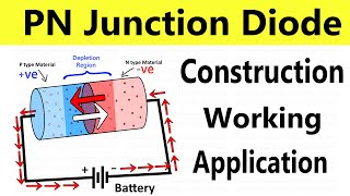
A PN junction is a critical semiconductor configuration that emerges when a p-type semiconductor, characterized by an abundance of holes, is joined with an n-type semiconductor, known for its high electron concentration. The point of connection is termed the junction, which acts as a diode—the fundamental component for numerous electronic devices.
Key Features
- P-Type Region: This area is rich in holes, which are the absence of electrons and act as positive charge carriers.
- N-Type Region: Here, electrons are the majority carriers, leading to a high density of negative charge.
- Junction: The interface created between these two regions is essential to the function of the junction diode.
Understanding the electrostatic properties of this junction, including the formation of a depletion region and an electric field, is fundamental for grasping how semiconductors operate in electronic circuits. The principles established by the PN junction extend into various practical applications, such as rectification, voltage regulation, and switching circuits.
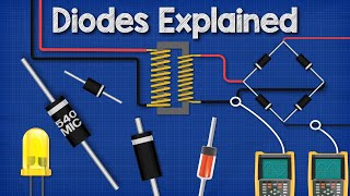
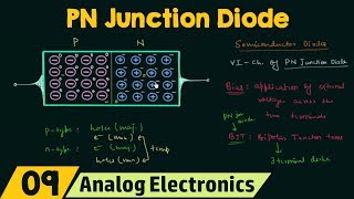
Youtube Videos
Audio Book
Dive deep into the subject with an immersive audiobook experience.
What is a PN Junction?
Chapter 1 of 2
🔒 Unlock Audio Chapter
Sign up and enroll to access the full audio experience
Chapter Content
A PN junction is formed when a p-type and n-type semiconductor are joined together, creating a junction diode. This is the fundamental building block of many electronic devices.
Detailed Explanation
A PN junction is a crucial component in electronics. It is created when two types of semiconductors, known as p-type and n-type, are combined. The p-type semiconductor has a high concentration of 'holes' (positive charge carriers), while the n-type semiconductor has a high concentration of electrons (negative charge carriers). When they are joined, a junction diode is formed, which is essential for many electronic operations, serving as the basis for devices like diodes and transistors.
Examples & Analogies
Think of a PN junction like a bridge between two towns. One town has a lot of positive residents (holes) eager to cross, while the other town is crowded with negative residents (electrons). When the bridge (the junction diode) is built, people from both towns can interact, creating important exchanges, just like how current flows through the PN junction in electronic devices.
Key Features of a PN Junction
Chapter 2 of 2
🔒 Unlock Audio Chapter
Sign up and enroll to access the full audio experience
Chapter Content
Key Features:
● p-type region: high hole concentration.
● n-type region: high electron concentration.
● Junction: boundary between p and n regions.
Detailed Explanation
The PN junction has distinct features that define its behavior in electronics. The p-type region is rich in holes, which are created by doping the semiconductor with elements that have fewer electrons. The n-type region, on the other hand, is doped with elements that have extra electrons. The 'junction' is the area where these two regions meet, and it plays a critical role in how the device operates. Understanding these features helps in grasping how diodes control the flow of electricity.
Examples & Analogies
Imagine a party where guests from two different groups (p-type and n-type) come together at a common place (the junction). The group with more 'empty spots' (p-type holes) meets those with more 'extra treats' (n-type electrons). This meeting point helps them interact and exchange ideas (or in the case of electronics, allows for the flow of current).
Key Concepts
-
PN Junction: The interface that forms when p-type and n-type semiconductors are joined.
-
P-Type Semiconductor: Higher concentration of holes creates positive charge carriers.
-
N-Type Semiconductor: Electron-rich area that provides negative charge carriers.
-
Depletion Region: The absence of mobile charge carriers near the junction leading to a built-in electric field.
Examples & Applications
In smartphones, PN junctions are used in diodes to ensure that current flows only in one direction, preventing damage to components.
In solar panels, PN junctions are critical as they generate electricity when exposed to sunlight.
Memory Aids
Interactive tools to help you remember key concepts
Rhymes
P-type brings the holes, n-type adds the streams, together they make junctions for electric dreams.
Stories
Imagine two islands, one filled with positive holes and the other with flowing electrons. When they meet, magic happens; they form a junction where energy flows in harmony.
Memory Tools
Remember 'P-N Dance' to recall that P-type and N-type semiconductors need to move together to create a PN junction.
Acronyms
Use 'PNE' to remember
P-type for Holes
N-type for Electrons.
Flash Cards
Glossary
- PN Junction
An interface created between p-type and n-type semiconductors, fundamental in the construction of diodes.
- PType Semiconductor
A semiconductor material that has an abundance of holes (positive charge carriers).
- NType Semiconductor
A semiconductor material that has a high concentration of electrons (negative charge carriers).
- Depletion Region
A region at the PN junction free of charge carriers, where an electric field is established.
- Electric Field
A field around the junction resulting from the separation of charge carriers in the depletion region.
Reference links
Supplementary resources to enhance your learning experience.