Reverse Bias
Enroll to start learning
You’ve not yet enrolled in this course. Please enroll for free to listen to audio lessons, classroom podcasts and take practice test.
Interactive Audio Lesson
Listen to a student-teacher conversation explaining the topic in a relatable way.
Understanding Reverse Bias
🔒 Unlock Audio Lesson
Sign up and enroll to listen to this audio lesson

Today, we will discuss reverse bias in PN junction diodes. Can anyone explain what happens when we apply reverse bias?

Isn't it when we connect the positive side to the n-type and negative to the p-type?

Exactly right! In this configuration, the depletion region widens, which increases the resistance to current flow. Can anyone tell me what this means for current flow?

It means that little to no current should flow, except maybe a tiny leakage current?

That's correct! The small leakage current is due to minority carriers. Let's remember that with the acronym MLP: Minimum Leakage current under Reverse Bias.
Characteristics of Reverse Bias
🔒 Unlock Audio Lesson
Sign up and enroll to listen to this audio lesson

Now let's delve into specific characteristics of diodes in reverse bias. What happens to the depletion region when we apply this bias?

It widens, reducing the flow of majority carriers.

Correct! The depletion region widens significantly, making it hard for electricity to flow. However, we do have a small leakage current. Why do we need to consider this leakage current?

It can affect the performance of circuits that use diodes, right?

Exactly! The leakage current can impact circuit operation, particularly in sensitive applications like signal processing.
Applications of Reverse Bias
🔒 Unlock Audio Lesson
Sign up and enroll to listen to this audio lesson

Finally, let's talk about applications. Can anyone name a situation where reverse bias is crucial?

In rectifiers to convert AC to DC!

That's one! In rectification, we need the diode to block current in the reverse direction to avoid damage. What else?

In protection circuits to prevent voltage spikes.

Exactly! We can use reverse bias to protect sensitive components. Remember this with the acronym RAMP: Reverse Bias Applications in Multi-Purpose electronics.
Introduction & Overview
Read summaries of the section's main ideas at different levels of detail.
Quick Overview
Standard
In reverse bias, the PN junction diode behaves as an insulator with only a minimal leakage current due to minority carriers. This behavior is crucial for understanding diode operations in various applications, where controlling current flow is paramount.
Detailed
Detailed Summary of Reverse Bias
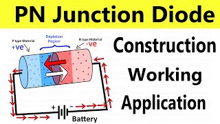
Reverse bias in a PN junction diode is characterized by applying the positive terminal of a voltage source to the n-type side and the negative terminal to the p-type side. This setup causes the depletion region to widen, inhibiting the flow of majority carriers (holes from p-type and electrons from n-type) across the junction. However, minority carriers (electrons in the p-side and holes in the n-side) can still move, resulting in a minimal leakage current that is typically negligible under normal conditions.
Key Points:
- Depletion Region Widening: The depletion region increases in width when reverse biased, significantly reducing the current flow through the diode.
- Leakage Current: Although minimal, a small leakage current exists due to the movement of minority carriers. This current is crucial for understanding the diode's behavior when reverse-biased.
- Diode Characteristics: Under reverse bias, the diode essentially acts as an insulator until a specific breakdown voltage is reached, after which the diode can conduct substantially.
- Applications: Understanding reverse bias is vital for applications where diodes need to block current in one direction while allowing a small reverse current, such as in rectifiers and protection circuits.
Youtube Videos


Audio Book
Dive deep into the subject with an immersive audiobook experience.
Definition of Reverse Bias
Chapter 1 of 2
🔒 Unlock Audio Chapter
Sign up and enroll to access the full audio experience
Chapter Content
● Positive terminal to n-side, negative to p-side.
● Depletion region widens.
● Very small leakage current flows due to minority carriers.
Detailed Explanation
Reverse bias occurs when the positive terminal of a voltage source is connected to the n-side of a PN junction and the negative terminal to the p-side. In this configuration, the internal electric field is enhanced, making the depletion region – the area devoid of free charge carriers – expand further. This widening further inhibits the flow of current across the junction. The only current that may flow is a small 'leakage current' caused by minority carriers (electrons in p-type and holes in n-type materials), which is typically negligible.
Examples & Analogies
Think of reverse bias like a one-way street designed to stop incoming traffic from the wrong direction. In normal operation, cars (electric current) can flow easily in one direction, but in reverse bias, it's as if the street is blocked for incoming cars, allowing only a few stray vehicles (minority carriers) to pass through.
Effects of Reverse Bias
Chapter 2 of 2
🔒 Unlock Audio Chapter
Sign up and enroll to access the full audio experience
Chapter Content
Condition Depletion Width Current Flow Junction
Behavior
Reverse Bias Increases Very Low Insulates
Detailed Explanation
When the PN junction is reverse biased, the depletion region's width increases. This phenomenon fundamentally alters the junction's behavior. Because of this increase in width, the ability of charge carriers to cross the junction is further restricted, leading to very low current flow. Hence, the diode effectively becomes an insulator, which is the desired behavior when preventing current flow in applications such as blocking reverse voltages in circuits.
Examples & Analogies
Imagine a dam that is built to hold back water (the electric current). When the dam is reinforced (reverse biasing the diode), it becomes harder for the water to pass through, which stays behind the dam (increased depletion width). This reinforces the dam's role as a barrier, thereby effectively insulating areas behind it.
Key Concepts
-
Depletion Region: The area in the PN junction where charge carriers are depleted, affecting conductivity.
-
Leakage Current: The minor current that flows even when the diode is reverse biased, primarily due to minority carriers.
-
Reverse Bias Applications: Reverse bias is essential in applications such as rectification and protection circuits.
Examples & Applications
Example 1: In a rectifier circuit, the diode must reverse bias during one half of the AC cycle to prevent current flow and ensure only one direction of current passes through, which is critical for AC to DC conversion.
Example 2: In a voltage protection circuit, a reverse-biased diode can prevent high voltage spikes from damaging sensitive components by blocking the reverse current.
Memory Aids
Interactive tools to help you remember key concepts
Rhymes
Wide the gap, no current clap; in reverse bias is where it maps.
Stories
Imagine a door (the diode) that only opens one way (forward bias). If you try to push it the other way (reverse bias), it not only stays shut but also lets a few curious passersby (minor carriers) slip through - but just a few!
Memory Tools
Think of 'RAMP': Reverse bias allows minimal passage.
Acronyms
Remember PIG
Positive to N-type
Increased Depletion
Guarded current (for reverse bias).
Flash Cards
Glossary
- Reverse Bias
A condition in a PN junction diode where the positive voltage is applied to the n-type side and negative to the p-type side, causing the depletion region to widen.
- Depletion Region
A zone around the PN junction devoid of charge carriers, resulting from the movement of electrons and holes.
- Leakage Current
A small amount of current that flows through a diode in reverse bias due to minority carriers.
Reference links
Supplementary resources to enhance your learning experience.
