
PN Junction Diode and Applications
Enroll to start learning
You’ve not yet enrolled in this course. Please enroll for free to listen to audio lessons, classroom podcasts and take practice test.
Interactive Audio Lesson
Listen to a student-teacher conversation explaining the topic in a relatable way.
Introduction to PN Junction
🔒 Unlock Audio Lesson
Sign up and enroll to listen to this audio lesson

Let's start with the basics of the PN junction diode. A PN junction is created when p-type and n-type semiconductors are joined together. Can anyone tell me what characterizes the p-type and n-type materials?

The p-type has a high concentration of holes, while the n-type has a high concentration of electrons!
Exactly! Those properties are crucial. This junction is essentially the foundation for many electronic devices. Think of it as a gate that allows current to flow in one direction but not the other.

So, why is it important to know about the junction?
Great question! Understanding the PN junction helps us to grasp how diodes function and their applications in circuits.
As a memory aid, remember 'P for positive holes' and 'N for negative electrons'.
Formation of Depletion Region
🔒 Unlock Audio Lesson
Sign up and enroll to listen to this audio lesson

Now, let's talk about the depletion region. When the p-type and n-type materials are joined, what happens to the electrons and holes?

Electrons from the n-side move to the p-side, and holes from the p-side move to the n-side!
Correct! This movement leaves behind fixed, immobile ions, forming the depletion region. Can anyone tell me what happens next?

An electric field is created across the junction, right?
Exactly! This electric field generates a built-in potential that influences how the diode behaves under bias conditions.
To remember this, think of it as 'deplete' when they diffuse. The area becomes 'depleted' of charge carriers.
Biasing of PN Junction
🔒 Unlock Audio Lesson
Sign up and enroll to listen to this audio lesson
We have two biasing conditions for our PN junction: forward bias and reverse bias. Who can explain what happens in forward bias?
In forward bias, the positive terminal is connected to the p-side, and the negative to the n-side, which narrows the depletion region!
Great job! And after we reach the threshold voltage, what happens?
Current flows easily!
That's correct! Now, what about reverse bias?
The positive terminal goes to the n-side, and the depletion region widens, leading to very low current flow!
Correct! Remember, in reverse bias, the diode acts as an insulator. Here's a mnemonic: 'R is for resistor' to help you recall this fact.
Applications of PN Junction Diode
🔒 Unlock Audio Lesson
Sign up and enroll to listen to this audio lesson
Now let's discuss applications! First, we have rectifiers. Can someone explain how a half-wave rectifier works?
It uses one diode and only allows one half of the AC cycle to pass!
Exactly! And how about a full-wave rectifier?
It can use two or four diodes to allow both halves of the AC cycle to output!
Great! Now we also have Zener diodes for voltage regulation. Remember, Zener diodes allow for a specific voltage to be maintained. What are some devices that use diodes?
We see them in LEDs, clipper circuits, and even solar cells!
Exactly! To summarize, remember: 'Rectify, Regulate, and Light' to capture the main applications of the PN junction diode.
Introduction & Overview
Read summaries of the section's main ideas at different levels of detail.
Quick Overview
Standard
This section explores the PN junction diode's formation, characteristics, biasing, current-voltage behavior (VI characteristics), and its applications in electronic devices. Key concepts such as forward and reverse bias, the depletion region, and diode operation equations are discussed to provide a comprehensive understanding.
Detailed
Detailed Summary of PN Junction Diode and Applications
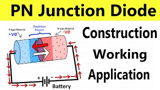
The PN junction diode is constructed from p-type and n-type semiconductors, creating a junction that serves as the basis for various electronic devices. The p-type region has a high hole concentration, while the n-type region has a high electron concentration, resulting in unique electrical properties.
The formation of a depletion region occurs when these materials are joined, leading to the diffusion of electrons and holes, which creates an electric field and a built-in potential.
In understanding how the diode operates, two primary biasing conditions are observed: forward bias (where current flows easily after a threshold voltage) and reverse bias (where the depletion region widens and current is minimal). The section touches on the key parameters governing how current behaves under these conditions, including the Shockley diode equation, which quantifies the relationship between current and voltage in ideal and real diodes.
The applications of diodes are diverse, ranging from rectifiers (AC to DC conversion) to voltage regulators and various optoelectronic devices like LEDs and photodiodes, making the PN junction diode crucial in modern electronics.
Youtube Videos


Audio Book
Dive deep into the subject with an immersive audiobook experience.
Introduction to PN Junction
Chapter 1 of 7
🔒 Unlock Audio Chapter
Sign up and enroll to access the full audio experience
Chapter Content
A PN junction is formed when a p-type and n-type semiconductor are joined together, creating a junction diode. This is the fundamental building block of many electronic devices.
Key Features:
● p-type region: high hole concentration.
● n-type region: high electron concentration.
● Junction: boundary between p and n regions.
Detailed Explanation
In this chunk, we learn about the PN junction, which is made by joining two types of semiconductors: p-type and n-type. The p-type semiconductor has a high concentration of holes (positive charge carriers), while the n-type has a high concentration of electrons (negative charge carriers). The area where these two materials meet is called the junction, and it is crucial as it forms the basic structure for various electronic devices, including diodes, transistors, and more.
Examples & Analogies
Think of the p and n regions as two teams: one team has a lot of players (holes) who can help score points, and the other team has a lot of fast runners (electrons) who can carry the ball. When they meet at the junction, they can create strong plays and strategies, which represent the functionality of a diode in electronic circuits.
Formation of Depletion Region
Chapter 2 of 7
🔒 Unlock Audio Chapter
Sign up and enroll to access the full audio experience
Chapter Content
● When p-type and n-type materials are joined, electrons diffuse from n to p, and holes diffuse from p to n.
● This movement leaves behind immobile ions, forming a depletion region (charge-free zone).
● An electric field is developed across the junction, creating a built-in potential (V₀).
Detailed Explanation
When the p-type and n-type semiconductors are connected, the electrons from the n-side naturally flow into the p-side, and the holes from the p-side flow to the n-side. This exchange occurs because electrons want to fill the holes. This movement of charge carriers results in an area without any free charges, called the depletion region. This region is significant because it acts as an insulator preventing current flow until a sufficient external voltage is applied. The movement of charges also creates an electric field at the junction, establishing a potential difference known as the built-in potential.
Examples & Analogies
Imagine a crowded room (the junction) where people (electrons and holes) are trying to find their places. As they move towards each other, some end up leaving empty chairs behind (creating the depletion region). This empty space becomes like a no-man's land until someone else comes with the right invitation (voltage) to fill those empty chairs and allow a conversation (current) to happen.
Biasing of PN Junction
Chapter 3 of 7
🔒 Unlock Audio Chapter
Sign up and enroll to access the full audio experience
Chapter Content
-
Forward Bias
● Positive terminal to p-side, negative to n-side.
● Depletion region narrows.
● Current flows easily after threshold voltage is reached. -
Reverse Bias
● Positive terminal to n-side, negative to p-side.
● Depletion region widens.
● Very small leakage current flows due to minority carriers.
Condition Depletion Width Current Flow Junction Behavior
Forward Bias Decreases High Conducts
Reverse Bias Increases Very Low Insulates
Detailed Explanation
Biasing of a PN junction relates to how an external voltage affects the behavior of the diode. In forward bias, connecting the positive terminal to the p-type side and the negative to the n-type side reduces the depletion region, allowing current to flow easily once a certain threshold voltage is exceeded (around 0.7V for silicon). Conversely, in reverse bias, where the positive terminal connects to the n-type side, the depletion region widens, and current flow is significantly suppressed except for a tiny leakage current caused by minority carriers. In summary, forward bias facilitates current flow, whereas reverse bias generally blocks it.
Examples & Analogies
Think of forward bias as opening a floodgate that allows water (current) to flow freely into a container (circuit). In contrast, reverse bias is like closing that gate and only allowing a small trickle (leakage current) through, which is manageable and doesn’t overflow the system.
VI Characteristics of PN Junction Diode
Chapter 4 of 7
🔒 Unlock Audio Chapter
Sign up and enroll to access the full audio experience
Chapter Content
Forward Bias:
● No current until threshold voltage (≈ 0.7 V for Si, 0.3 V for Ge).
● Beyond this, current increases exponentially.
Reverse Bias:
● Current is almost zero until breakdown voltage is reached.
● After breakdown, current increases sharply.
Detailed Explanation
The VI characteristics of a PN junction diode show how current (I) varies with applied voltage (V). In forward bias, there’s a threshold voltage (typically 0.7 volts for silicon) that must be overcome before current can flow. Once this threshold is surpassed, the current rises sharply in an exponential manner. In reverse bias, the diode ideally prevents current flow until a critical reverse voltage called breakdown voltage is reached, at which point the diode conducts sharply due to breakdown effects.
Examples & Analogies
Imagine a water pipe: initially, there is no water flowing until the pressure builds up to a certain point (threshold voltage). Once that point is passed, the pressure causes a swift flow of water (current). In reverse, it's like trying to suck water back through the pipe: a tiny amount will escape under light pressure (leakage current), but nothing substantial happens until a stronger force (breakdown voltage) pushes it through.
Diode Equation
Chapter 5 of 7
🔒 Unlock Audio Chapter
Sign up and enroll to access the full audio experience
Chapter Content
The current II through a PN junction is given by the Shockley Diode Equation:
I=Is(eqVnkT−1)I = I_s \left( e^{\frac{qV}{nkT}} - 1 \right)
Where:
● II: diode current
● IsI_s: reverse saturation current
● qq: electronic charge
● VV: applied voltage
● nn: ideality factor (typically 1-2)
● kk: Boltzmann constant
● TT: absolute temperature
Detailed Explanation
The Shockley diode equation provides a mathematical relationship for calculating the current flowing through a diode based on various parameters. 'I' represents the actual current through the diode, 'I_s' is the reverse saturation current, and 'V' is the voltage across the diode. The equation indicates that the current increases exponentially with applied voltage, which shows the diode's sensitivity to small changes in voltage.
Examples & Analogies
You could think of this equation like a thermostat where minor changes in temperature (voltage) can lead to significant changes in the heating system's activity (current). Just as a small temperature change can turn the heat on or off in a room, a slight voltage change can dramatically affect the current through a diode.
Ideal vs Real Diode
Chapter 6 of 7
🔒 Unlock Audio Chapter
Sign up and enroll to access the full audio experience
Chapter Content
Parameter Ideal Diode Real Diode
Threshold Voltage 0 V 0.3 V (Ge), 0.7 V (Si)
Reverse Leakage 0 A Small current
Reverse Infinite Occurs at certain Breakdown voltage
Detailed Explanation
This chunk compares ideal diodes, which are theoretical devices that have no threshold voltage or reverse leakage, with real diodes that exist in practice. Real diodes need a certain amount of voltage to start conducting (threshold voltage) and exhibit small leakage currents even when they should ideally be turned 'off'. Additionally, real diodes can break down at certain conditions, unlike ideal ones which do not.
Examples & Analogies
Consider ideal diodes as perfect light switches that work flawlessly without resistance or delay, while real diodes are like regular light switches that might experience flicker or require a little pressure to turn on but still do the job well enough in everyday use.
Applications of PN Junction Diode
Chapter 7 of 7
🔒 Unlock Audio Chapter
Sign up and enroll to access the full audio experience
Chapter Content
- Rectifiers
● Convert AC to DC.
a. Half Wave Rectifier
● Uses one diode.
● Output only for one half of the AC cycle.
b. Full Wave Rectifier
● Uses two or four diodes (center-tap or bridge).
● Output in both halves of the AC cycle. - Clippers and Clampers
● Modify the shape of input signals. - Voltage Regulation
● With Zener diode, provides constant voltage. - Switching Circuits
● Used in logic gates and digital circuits.
Detailed Explanation
PN junction diodes are versatile components used in various applications. Firstly, they are essential in rectifiers, devices that convert alternating current (AC) to direct current (DC). Half-wave rectifiers utilize one diode and only allow half of the AC signal to pass, while full-wave rectifiers can use multiple diodes to utilize both halves of the AC signal, making them more efficient. Moreover, diodes can act as clippers or clampers that alter the shape of input signals, and Zener diodes specifically are employed for regulating voltage to provide stability in electrical circuits. Lastly, diodes are fundamental in switching circuits used in digital logic gates.
Examples & Analogies
Imagine using a water tap (rectifier) to control water flow (electricity). A half-wave tap lets water flow only in one direction, while a full-wave tap allows water to flow in both directions efficiently. Similarly, Zener diodes can be thought of as pressure regulators ensuring that the water pressure (voltage) remains constant, providing a steady output for various uses.
Key Concepts
-
PN Junction: The formation of a boundary between p-type and n-type semiconductors.
-
Depletion Region: The area where charge carriers are depleted, forming an electric field.
-
Biasing: The application of voltage to a diode, affecting current flow.
-
Forward Bias: A condition that allows significant current flow when threshold voltage is met.
-
Reverse Bias: A condition that results in minimal current, acting as an insulator.
-
Applications: Includes rectifiers, voltage regulators, and optoelectronic devices.
Examples & Applications
In a half-wave rectifier configuration, one diode allows current to pass only during the positive half-cycles of the AC input.
A Zener diode regulates voltage by allowing current to flow in reverse at a specified voltage, keeping the output voltage stable.
Memory Aids
Interactive tools to help you remember key concepts
Rhymes
In forward bias, current flows with ease, but reverse makes it seem like a freeze.
Stories
Imagine a gate that only opens when a certain key is used. That’s the PN junction where only the right voltage allows current through.
Memory Tools
Remember 'F for flow' during forward bias and 'R for resist' during reverse bias.
Acronyms
To remember diode applications
RAP (Rectification
Voltage Regulation
and Optoelectronics).
Flash Cards
Glossary
- PN Junction
The boundary formed when a p-type and n-type semiconductor are joined together.
- Depletion Region
A charge-free zone resulting from the diffusion of electrons and holes in a PN junction.
- Forward Bias
Condition where the positive terminal is connected to the p-side, allowing current to flow after the threshold voltage.
- Reverse Bias
Condition where the positive terminal is connected to the n-side, resulting in minimal current flow.
- Shockley Diode Equation
Equation that describes the current through a PN junction in terms of applied voltage and material constants.
- Rectifiers
Devices that convert alternating current (AC) to direct current (DC).
- Zener Diode
A diode designed to operate in reverse breakdown to provide voltage regulation.
- Light Emitting Diode (LED)
A special diode that emits light when forward biased.
- Photodiode
A diode that generates current when exposed to light.
Reference links
Supplementary resources to enhance your learning experience.