
Voltage Model
Enroll to start learning
You’ve not yet enrolled in this course. Please enroll for free to listen to audio lessons, classroom podcasts and take practice test.
Interactive Audio Lesson
Listen to a student-teacher conversation explaining the topic in a relatable way.
Introduction to Small Signal Equivalent Circuit
🔒 Unlock Audio Lesson
Sign up and enroll to listen to this audio lesson

Today we start discussing the small signal equivalent circuit, specifically for the Common Source Amplifier. Can anyone tell me why we set the DC bias to zero?

Is it to focus on the AC signals?
Exactly! It simplifies our analysis by allowing us to only consider small fluctuations around the bias point. So, if we have a signal, what is usually used to relate the output to the input?

The voltage gain, right?
Correct! We denote it as A = -g_m * R_D. Who remembers what g_m stands for?

Transconductance, which indicates how effectively the amplifier converts input voltage to output current.
Great job! To summarize, setting the DC bias to zero allows us to focus on small signal behavior, and we use the transconductance to quantify how effectively we gain amplification.
Calculating Output Resistance
🔒 Unlock Audio Lesson
Sign up and enroll to listen to this audio lesson

Now, let's discuss how to find the output resistance, R_O. Can anyone remind me how we usually approach this?

Do we look from the output side and see the current that flows through the resistances?
Exactly! By observing the circuit from the output port and applying voltage across it while keeping other inputs grounded, we can determine R_O. What relationship do we express this with?
It’s v_x = R_O * i_x.
Perfect! Remember that R_O is crucial as it helps define the interaction between our amplifier and the load it drives.
Input Resistance Calculation
🔒 Unlock Audio Lesson
Sign up and enroll to listen to this audio lesson
Let’s move on to calculating the input resistance, R_in. What do we need to consider here?
We examine the configuration when the gate current is zero?
That's right! So, when the gate current is zero, we assume that R_in is mostly due to the parallel combination of the resistances we see. What do we express this as?
It’s R_in = R_1 || R_2, where R_1 and R_2 are the resistances at the input.
Excellent! This input resistance affects how the amplifier interacts with previous stages. Let’s summarize: Determining R_in relies on assuming zero current at the gate, allowing us to consider the parallel resistance effect.
Impact of Parasitic Capacitance
🔒 Unlock Audio Lesson
Sign up and enroll to listen to this audio lesson
Finally, let’s touch on high frequency scenarios and parasitic capacitances. Why are these important?
They can significantly affect the performance of the amplifier, especially in high frequency applications.
Correct! Parasitic capacitances like C_gs and C_gd can introduce delays and distort the signal. How does this relate to the Miller effect?
The Miller effect can make the input capacitance appear larger, which affects the frequency response.
Exactly! Remember, in the presence of these capacitances, calculating the voltage gain and determining frequency response requires careful consideration of these effects. Let’s recap: Parasitic capacitances can alter performance, and the Miller effect compounds the impact by increasing the effective capacitance seen at the input.
Introduction & Overview
Read summaries of the section's main ideas at different levels of detail.
Quick Overview
Standard
This section explains the Voltage Model in the context of a Common Source Amplifier. It details the small signal equivalent circuit, calculations of voltage gain, output resistance, and input resistance, along with the importance of DC biasing and the effects of parasitic capacitance in high frequency situations.
Detailed
Voltage Model
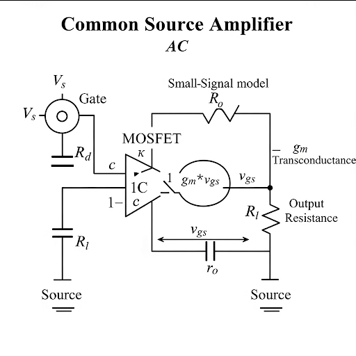
The Voltage Model involves mapping the small signal equivalent circuit of a Common Source Amplifier. The fundamental steps include: 1. Setting DC bias to zero, thus focusing exclusively on AC signals. 2. Identifying the voltage gain, which is obtained from the relationship between output voltage and input voltage. This is denoted as A = -g_m * R_D, where g_m is the transconductance and R_D is the drain resistance.
Next, the section addresses the calculation of output resistance (R_O) by observing the circuit from the output port, enabling us to relate the voltage at the output to the current through the resistance. The input resistance (R_in) is calculated by examining the circuit configuration at the input port.
The implications of high frequency signals are also discussed, highlighting the effects of parasitic capacitances and how they can affect amplifier performance, particularly in relation to the Miller effect. Finally, a numerical example illustrates how to calculate voltage gain using given parameters, showcasing the practical application of the Voltage Model.
Youtube Videos

Audio Book
Dive deep into the subject with an immersive audiobook experience.
Voltage Gain of the Amplifier
Chapter 1 of 6
🔒 Unlock Audio Chapter
Sign up and enroll to access the full audio experience
Chapter Content
So, that gives us the voltage gain A defined as v_out/v_in = -R_D * g_m. So, this is the first parameter of the voltage amplifier namely the voltage gain.
Detailed Explanation
The voltage gain (A) of an amplifier is defined as the ratio of the output voltage (v_out) to the input voltage (v_in). In this case, the voltage gain is represented by the formula A = -R_D * g_m. Here, R_D is the resistance at the output, and g_m is the transconductance parameter of the amplifier. The negative sign indicates that the output voltage is inverted compared to the input.
Examples & Analogies
Think of a voltage amplifier like a see-saw where one side goes up while the other side goes down. If you push down on one end (input voltage), the other end (output voltage) will rise to a new level, but it may do so inversely, which is why we get the negative sign in the formula.
Output Resistance
Chapter 2 of 6
🔒 Unlock Audio Chapter
Sign up and enroll to access the full audio experience
Chapter Content
So, that makes this current 0 and then if you stimulate this output port by say v_x and then if you observe the corresponding current here as i_x. In fact, the current it is only going through this resistance. So, then v_x and the i relationship you will get is basically v_x = R_D * i_x.
Detailed Explanation
To understand the output resistance of the amplifier, you apply a voltage v_x at the output while ensuring that the input is terminated (current is set to zero). The output voltage (v_x) is then directly proportional to the output current (i_x) flowing through the output resistance (R_D). This can be expressed as v_x = R_D * i_x, highlighting the relationship between voltage, current, and resistance.
Examples & Analogies
Imagine trying to push water out of a garden hose. The resistance (R_D) in the hose affects how much water flows out (current). The more you push (voltage), the more water comes out, but the amount that actually comes out is affected by the resistance of the hose.
Input Resistance
Chapter 3 of 6
🔒 Unlock Audio Chapter
Sign up and enroll to access the full audio experience
Chapter Content
At the input port if we see and if you see what is the corresponding resistance here... that gives us the expression v_s = (R_1 || R_2).
Detailed Explanation
The input resistance of the amplifier is determined by looking at the resistance at the input port when no current is flowing into it (the gate current is assumed to be zero). We can evaluate the input resistance as the parallel combination of resistances R_1 and R_2. The formula v_s = (R_1 || R_2) shows that the input voltage (v_s) can be expressed as a function of these parallel resistances.
Examples & Analogies
Think of two parallel water slides at a park. When kids slide down, they choose either slide (R_1 or R_2). If both slides are available, more kids can slide down simultaneously, similar to how resistors in parallel share the current, affecting the total input resistance.
Transconductance Amplifier Relation
Chapter 4 of 6
🔒 Unlock Audio Chapter
Sign up and enroll to access the full audio experience
Chapter Content
Now, as we have given a hint that since the main circuit this current is 0 before we start considering the input capacitance... G = AV/m, therefore relates the transconductance G and the voltage gain A.
Detailed Explanation
In scenarios where the current into the input port is negligible, we can treat the amplifier as a transconductance amplifier. Here, the relationship between the transconductance (G) and the voltage gain (A) is defined mathematically as G = A * V/m, relating the two in terms of output current dependence on input voltage.
Examples & Analogies
Think of a volume control knob on a stereo. When you turn the knob (input voltage), it determines how much loud the stereo plays (output current). The knob adjusts the amplifier's behavior much like the transconductance describes how a small input voltage affects the larger output current.
High Frequency Effects
Chapter 5 of 6
🔒 Unlock Audio Chapter
Sign up and enroll to access the full audio experience
Chapter Content
Now, if we consider the high frequency situation... include the effect of λ, then at the output side it may be having finite conductance.
Detailed Explanation
When analyzing circuits at high frequencies, additional factors such as parasitic capacitances and finite conductance need to be taken into consideration. In this context, as frequency increases, the characteristics of the amplifier change due to these parasitic effects, affecting the overall performance and gain of the output signal.
Examples & Analogies
Consider trying to fill a balloon with air (high frequency) through a tiny straw. As the frequency of filling increases, you encounter resistance not just from the straw size (pulling air through a small opening) but also from the balloon material stretching and pushing back (parasitic capacitances). Both constraints together can limit how quickly the balloon can be filled.
Cutoff Frequencies
Chapter 6 of 6
🔒 Unlock Audio Chapter
Sign up and enroll to access the full audio experience
Chapter Content
So, as a result the previous analysis it was valid in the mid frequency region... the role of this C and C in the frequency response.
Detailed Explanation
The amplifier has defined cutoff frequencies, namely a lower cutoff and an upper cutoff frequency based on its RC time constants. Understanding these cutoff frequencies is essential as they define the range of frequencies over which the amplifier operates optimally. Any signal or input outside of these frequencies will be attenuated, affecting how the amplifier can be used in practical applications.
Examples & Analogies
Think of a concert speaker system that is tuned to work best within certain frequencies. If you play music that is too bass-heavy (lower cutoff frequency) or too treble-heavy (upper cutoff frequency), the speaker may not sound as good. Just like the speaker has a range in which it performs best, amplifiers have their ranges of optimal frequency response.
Key Concepts
-
Voltage Gain: The amplification factor that defines the ratio of output voltage to input voltage.
-
Transconductance (g_m): A parameter that quantifies an amplifier's ability to convert input voltage variations into output current changes.
-
Output Resistance (R_O): A critical component that indicates how well the amplifier can drive different loads.
-
Input Resistance (R_in): Determines how the amplifier interacts with signal sources and prior stages.
-
Parasitic Capacitance: Unintentional capacitance that can cause signal degradation, particularly at high frequencies.
-
Miller Effect: A phenomenon that enlarges the effective input capacitance due to feedback within an amplifier circuit.
Examples & Applications
Example 1: For a common source amplifier with R_D = 3kΩ and g_m = 2mA/V, the voltage gain (A) can be calculated as A = -g_m * R_D = -2mA/V * 3kΩ = -6.
Example 2: If a voltage signal of 120mV is applied to a common source amplifier with a voltage gain of -6, the expected output signal would be approximately -720mV.
Memory Aids
Interactive tools to help you remember key concepts
Rhymes
When voltage gain is quite a feat, negative g_m makes outputs neat.
Stories
Imagine a tiny signal in a circuit, it whispers to transconductance to amplify its dreams; with the help of resistances, it blossoms, becomes large, but beware the parasitics lurking nearby.
Memory Tools
Remember the acronym V-GROW: V for Voltage gain, G for g_m, R for Resistance, O for Output resistance, W for Wattage.
Acronyms
Remember AMP
for Amplifier
for Mosfet
for Performance.
Flash Cards
Glossary
- Voltage Gain
The ratio of output voltage to input voltage in an amplifier, often expressed as a negative value in the context of inverting amplifiers.
- Transconductance (g_m)
A measure of the sensitivity of the output current of a device to its input voltage; it is represented in milliamperes per volt (mA/V).
- Output Resistance (R_O)
The resistance seen by the output of the amplifier, which affects how it drives connected loads.
- Input Resistance (R_in)
The resistance seen by the input of the amplifier, essential for understanding signal interaction with preceding stages.
- Parasitic Capacitance
Unintended capacitances within electronic components that can influence performance, particularly at high frequencies.
- Miller Effect
A phenomenon where the effective input capacitance increases due to feedback from the output, impacting amplifier behavior at high frequencies.
Reference links
Supplementary resources to enhance your learning experience.