
Small Signal Equivalent Circuit
Enroll to start learning
You’ve not yet enrolled in this course. Please enroll for free to listen to audio lessons, classroom podcasts and take practice test.
Interactive Audio Lesson
Listen to a student-teacher conversation explaining the topic in a relatable way.
Understanding the Small Signal Model
🔒 Unlock Audio Lesson
Sign up and enroll to listen to this audio lesson

Today we will discuss the small signal equivalent circuit for our Common Source Amplifier. To start, what do you think happens if we ignore the D.C. component?

I think it allows us to focus on the small changes in AC signals.
Exactly! By zeroing the D.C. bias, we can simplify our analysis. We replace the MOSFET with its small signal model. Does anyone remember how to determine the voltage gain?

Is it the formula A = -R_D * g_m?
Correct! Remember, g_m is the transconductance. It defines the channel's responsiveness to the input voltage. Now, what happens to output voltage in this small signal model?

The output voltage would be influenced directly by the small signal current flowing through the output resistor.
That's right! The output voltage can be expressed as V_out = -R_D * i_small. Let's keep this in mind as we proceed.
Key Parameters in the Small Signal Analysis
🔒 Unlock Audio Lesson
Sign up and enroll to listen to this audio lesson

Let's dive deeper into the parameters for our small signal model. We have the voltage gain, output resistance, and input resistance. Can anyone define the output resistance?

The output resistance is what we measure at the output terminals when the input signal is zeroed.
Great! So, when we stimulate an output port and measure current, we can represent this in terms of voltage over current, which leads us to define it as R_O. What about the input resistance?
Since the gate current is ideally zero, the input resistance is just based on the resistive elements connected to that gate!
Exactly! You all are doing well. Just remember that in amplifiers, these resistances help determine how they interact with other components.
Voltage and Transconductance Amplifiers
🔒 Unlock Audio Lesson
Sign up and enroll to listen to this audio lesson
Now that we've discussed the voltage gain and input/output resistances, let's talk about configurations. Can anyone explain how voltage and transconductance amplifiers differ?
A voltage amplifier outputs a voltage across its load while a transconductance amplifier outputs current.
Right! In terms of components, can you recall what changes in terms of models we use?
Yes! We use a different output model, G * v for transconductance, compared to A * v for voltage amplifiers.
Perfectly put! By manipulating these components, we can create versatile circuits suitable for various applications.
Frequency Response Considerations
🔒 Unlock Audio Lesson
Sign up and enroll to listen to this audio lesson
We need to consider frequency response next. What challenges can occur at low and high frequencies in our circuit?
Low frequencies might get affected by coupling capacitors and lead to a cutoff effect.
Exactly! Those capacitors can limit the signal passing through. What about at higher frequencies?
The parasitic capacitances, like gate to source, could introduce additional reactance.
Spot on! These reactances can influence our gain and frequency response. It's crucial to identify and factor them into our designs.
Numerical Analysis and Practical Implications
🔒 Unlock Audio Lesson
Sign up and enroll to listen to this audio lesson
Finally, let’s look at a numerical problem involving the Common Source Amplifier. What is the first step in calculating the gain?
We should calculate the DC operating point first, considering the bias components.
Exactly! After determining the quiescent current, how do we move on to finding g_m?
By applying the equation g_m = k * (V_GS - V_th), right?
That's correct. And remember, ultimately our gain is found using A = -g_m * R_D. It’s so important that we trace these steps methodically!
Introduction & Overview
Read summaries of the section's main ideas at different levels of detail.
Quick Overview
Standard
In this section, we delve into the small signal equivalent circuit for a Common Source Amplifier, detailing how to analyze it by zeroing the DC components. Key parameters including voltage gain, output resistance, and the definition of input resistance are covered, along with the impact of small signal analysis.
Detailed
Small Signal Equivalent Circuit
The small signal equivalent circuit is a vital concept in the analysis of amplifiers, especially for the Common Source Amplifier. In this section, we begin by establishing a zero-D.C. bias condition, allowing us to focus on the small signal analysis which ignores the direct current biasing. After zeroing the DC components and shorting the capacitors, we derive key expressions related to the amplifier performance.
Key Parameters
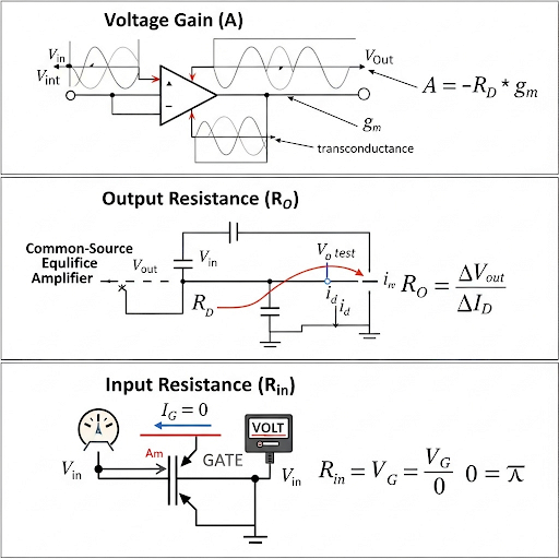
- Voltage Gain (A): The output voltage over the input voltage ratio, calculated as A = -R_D * g_m, where R_D is the drain resistance and g_m is the transconductance.
- Output Resistance (R_O): When the output is analyzed by applying a small input signal, the output resistance can be derived based on the relationship of output voltage and current flowing through the drain.
- Input Resistance (R_in): Defined in the open-circuit condition at the gate of the transistor, where gate current is ideally zero. The input resistance is influenced by the configuration of resistors connected to the input.
Significance
Understanding these parameters helps in effectively designing and analyzing circuits for desired amplifier characteristics, especially in applications like VLSI where MOSFETs are common.
Youtube Videos

Audio Book
Dive deep into the subject with an immersive audiobook experience.
Introduction to the Small Signal Equivalent Circuit
Chapter 1 of 7
🔒 Unlock Audio Chapter
Sign up and enroll to access the full audio experience
Chapter Content
Welcome back after the short break and we are about to start the small signal equivalent circuit for the Common Source Amplifier.
In the small signal equivalent circuit first thing is that we are making the DC bias to be 0. And then the capacitor we have sorted here and the capacitor we have sorted here...
Detailed Explanation
This introduction sets the stage for understanding the small signal equivalent circuit of a Common Source Amplifier. The key point is that during small signal analysis, DC bias levels are set to zero to simplify the calculations. This allows us to focus purely on how the circuit behaves with small variations in input signal voltage, without the influence of DC conditions.
Examples & Analogies
Imagine you are tuning a musical instrument. Before you start playing, you may want to tune it to a standard pitch (like A440) before you explore how it sounds under different notes. The same way, setting the DC bias to zero lets us analyze the circuit's response to small signals (the different notes) without the 'background noise' of the DC voltage (the tuning).
Analyzing Output Voltage and Voltage Gain
Chapter 2 of 7
🔒 Unlock Audio Chapter
Sign up and enroll to access the full audio experience
Chapter Content
Let me write the expression of this v_out, it is v_out = - R_D × g_m × v_gs. This leads to the voltage gain A defined as A_v = v_out / v_in.
Detailed Explanation
The output voltage can be expressed in terms of the drain resistor (R_D), transconductance (g_m), and the gate-source voltage (v_gs). This formulation shows that the output voltage is negatively proportional to the input voltage when multiplied by the gain factor (-R_D × g_m). The voltage gain A is a crucial parameter that indicates how much the input signal is amplified at the output.
Examples & Analogies
Think of a microphone connected to a speaker. The microphone picks up a faint sound (input), and the speaker amplifies it to a level that can be heard by a crowd (output). The efficiency of this amplification can be compared to the voltage gain in the amplifier circuit.
Output Resistance and Input Resistance
Chapter 3 of 7
🔒 Unlock Audio Chapter
Sign up and enroll to access the full audio experience
Chapter Content
The second parameter it is the output resistance. While we will be doing this, we can connect a signal source here and make this part equals to 0...
Detailed Explanation
Understanding both the output resistance and input resistance is vital for analyzing how the amplifier interacts with other circuits. Output resistance is measured by connecting a testing signal source and determining how much current is generated for a particular output voltage. At the input, resistance is considered to be high (essentially infinite) because the gate current is assumed to be zero.
Examples & Analogies
Consider a garden hose. The hose's thickness affects the flow of water through it when pressure is applied. Similarly, the input and output resistances influence how well signals can flow through the amplifier's circuit paths.
Transconductance Amplifier vs. Voltage Amplifier
Chapter 4 of 7
🔒 Unlock Audio Chapter
Sign up and enroll to access the full audio experience
Chapter Content
We can say that the signal at this input port it will be always in the form of voltage. On the other hand, the output port can be either voltage or current, referred to as a transconductance amplifier.
Detailed Explanation
This describes the dual nature of the amplifier – it can function as either a voltage amplifier or a transconductance amplifier, depending on how the signals are applied. While the input is typically a voltage, the output can either reflect this voltage or convert it to a current signal.
Examples & Analogies
Think of a power outlet in your home. The outlet provides electrical energy that can either power a lamp (acting like a voltage amplifier) or charge a phone (where the flow of current is emphasized, like a transconductance amplifier).
High Frequency Considerations
Chapter 5 of 7
🔒 Unlock Audio Chapter
Sign up and enroll to access the full audio experience
Chapter Content
Now, if we consider the high-frequency situation, namely if we consider the signal you are feeding here it is in the high frequency range...
Detailed Explanation
When dealing with high-frequency signals, we need to consider additional parameters such as parasitic capacitances. These unwanted capacitances can affect circuit performance drastically, leading to variations in the gain and response of the amplifier. Additionally, the output conductance must be considered when analyzing circuits that are operating at high frequencies.
Examples & Analogies
Imagine trying to track a fast-moving car with a camera. If your camera isn’t fast enough to keep up, you might get a blurry image. Similarly, if the amplifier can't handle high-frequency signals, its output will become distorted, impacting its effectiveness.
Low Frequency and Cutoff Frequencies
Chapter 6 of 7
🔒 Unlock Audio Chapter
Sign up and enroll to access the full audio experience
Chapter Content
The lower cutoff frequency it will be defined by f_cutoff(L) = 1 / (2π(R1∥R2) × C1).
Detailed Explanation
Cutoff frequencies help determine the frequency range over which the amplifier operates effectively. The lower cutoff frequency occurs due to capacitive effects and informs us about the lowest signal frequency that can pass through the amplifier with acceptable gain. As frequency increases or decreases beyond these points, gain diminishes significantly.
Examples & Analogies
Think of a filter you use for brewing coffee. It only allows certain sizes of coffee grounds to pass through, much like how cutoff frequencies allow certain frequency signals. Anything too high or too low gets filtered out, resulting in a less flavorful cup of coffee just as a weak electrical signal might result from a poorly designed amplifier.
Summary and Practical Implications
Chapter 7 of 7
🔒 Unlock Audio Chapter
Sign up and enroll to access the full audio experience
Chapter Content
So, we have discussed about the mapping to small signal equivalent circuit and then biasing and all more from the analysis point of view.
Detailed Explanation
This summary encapsulates the primary points discussed in the section, including how the small signal equivalent circuit is analyzed and what practical implications these factors have on designing and optimizing amplifiers. Concepts like biasing, resistance, gain, and frequency response were emphasized as foundational to understanding how amplifiers function.
Examples & Analogies
Consider designing a car engine: understanding the small parts like spark plugs and fuel injectors while also seeing how they work together to make the engine run efficiently is similar to how this analysis looks at the amplifier's components and their impact on performance.
Key Concepts
-
Small Signal Analysis: A method of examining amplifier behavior under small variations without considering DC components.
-
Voltage Gain: An important parameter indicating how effectively an amplifier increases input signal strength, typically calculated as A = -g_m * R_D.
-
Input and Output Resistance: Key resistive components that affect amplifier performance, influencing how they interact with connected circuits.
Examples & Applications
The small signal voltage gain for a given Common Source Amplifier can be calculated using a specified transconductance and drain resistance.
If the output current is defined as -g_m * V_in, and given parameters are known, one can determine the output voltage response under small signal conditions.
Memory Aids
Interactive tools to help you remember key concepts
Rhymes
For each signal's call, learn the small ones all; voltage, gain, and resistance too, will help your circuits pass right through.
Stories
Imagine a small signal running through a circuit, ignoring the noise of a big DC voltage. It weaves through resistances, gaining strength until it reaches the output, where it shows off its power.
Memory Tools
G.A.I.N. - Gain = A = -g_m * R_D, where G represents Gain, A is the formula, I is for input, and N is the output.
Acronyms
R.A.G.E. - R for Resistance, A for Amplifier, G for Gain, E for Equivalent circuit. Together they help us remember the components in our study.
Flash Cards
Glossary
- Small Signal Model
An analytical approach that simplifies the analysis of amplifiers by considering only the small variations in input signals, ignoring DC components.
- Voltage Gain (A)
The ratio of output voltage to input voltage in an amplifier, often expressed as a negative value for inverting amplifiers.
- Transconductance (g_m)
A parameter representing the relationship between the output current and the input voltage in a transistor, indicative of amplifier performance.
- Output Resistance (R_O)
The resistance seen by the output signal of the amplifier, widely determined by the external components and the intrinsic properties of the transistor.
- Input Resistance (R_in)
The resistance presented by the amplifier's input terminals which influences how it interacts with the preceding components in the circuit.
Reference links
Supplementary resources to enhance your learning experience.