
Advantages of FinFET Technology
Interactive Audio Lesson
Listen to a student-teacher conversation explaining the topic in a relatable way.
Better Electrostatic Control
🔒 Unlock Audio Lesson
Sign up and enroll to listen to this audio lesson

Today we'll explore how FinFETs provide better electrostatic control compared to traditional planar MOSFETs. Can anyone remind me what electrostatic control refers to?

Is it about how the gate voltage affects the channel?
Exactly! In FinFETs, the three-dimensional structure helps in reducing drain-induced barrier lowering, or DIBL. Why is this reduction important?

Because it improves the overall performance of the transistor?
Correct! It also increases immunity to short-channel effects which are critical as we scale down technology nodes. Let’s use the acronym 'HEM' to remember: Higher Electrostatic control, immunity to short-channel Effects, and Minimized DIBL. Can anyone summarize this?

FinFET has better control because of its structure, reducing unwanted electrical effects.
Great summary! Remember, improved electrostatic control is crucial for enhancing performance in smaller nodes.
Lower Leakage Current
🔒 Unlock Audio Lesson
Sign up and enroll to listen to this audio lesson

Next, let’s look at leakage currents. Who can explain what leakage current is?

It’s the unwanted current that flows even when a device is off, right?
Exactly! FinFETs achieve lower leakage currents through a thicker effective gate oxide. How does that benefit the overall device?
It reduces power consumption?
Yes! Lower leakage current means better efficiency. Let’s remember 'Less is More' for leakage currents: Less leakage leads to More efficiency. Who can summarize this concept?
FinFETs have lower leakage current due to thicker gate oxide, leading to higher efficiency.
High Drive Current and Speed
🔒 Unlock Audio Lesson
Sign up and enroll to listen to this audio lesson
Let’s delve into the drive current and speed of FinFETs. Can someone explain what drive current means?
I think it's the current that helps drive the device’s operation.
Exactly! The fin structure allows for an increased effective channel width, which boosts this drive current. What does that mean for speed?
It means faster switching, right?
Spot on! Faster switching improves the frequency response. Remember 'FIN' for Drive Current: 'F' for Faster switching, 'I' for Increased width, and 'N' for Notable performance!
Lower Power Consumption
🔒 Unlock Audio Lesson
Sign up and enroll to listen to this audio lesson
Next, let’s discuss power consumption. Why is lower power consumption critical in today's tech?
To extend battery life in portable devices!
Exactly! FinFETs can operate at lower supply voltages. Can anyone explain how this improves performance-per-watt?
Lower voltage means we can save power, improving efficiency during operations.
Very well put! Let’s do a mnemonic for this: 'Power Optimized, Performance Enhanced' – it summarizes how FinFETs improve both. Quick recap?
FinFETs save power by operating at lower voltages and improving performance metrics.
Scalability
🔒 Unlock Audio Lesson
Sign up and enroll to listen to this audio lesson
Lastly, let’s discuss scalability. Why is scalability important in semiconductor technology?
It allows for continued miniaturization of circuits, right?
Precisely! FinFETs are suitable for nodes below 14 nm, making them vital for modern processors. How does this position FinFETs against traditional MOSFETs?
They are much more efficient for smaller nodes and future technologies!
Excellent! Let’s summarize with 'FINS' for Future Innovations in Nano-Scale technology: FinFETs pave the way for future innovations through superior scalability.
Introduction & Overview
Read summaries of the section's main ideas at different levels of detail.
Quick Overview
Standard
FinFET technology has revolutionized the semiconductor industry by providing significant advantages such as enhanced gate control resulting in reduced short-channel effects, lower leakage currents, and higher performance metrics. These benefits make FinFETs suitable for advanced technology nodes below 14nm.
Detailed
Advantages of FinFET Technology
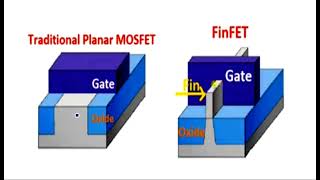
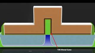
The introduction of Fin Field Effect Transistors (FinFETs) marks a paradigm shift in semiconductor technology. As transistor dimensions shrink, achieving better control over electrical properties becomes critical. FinFETs, with their unique three-dimensional structure, provide distinct benefits:
1. Better Electrostatic Control
- Reduced Drain-Induced Barrier Lowering (DIBL): FinFETs exhibit improved control over the channel, minimizing the unwanted electrical interactions that lead to DIBL, a key issue in small geometry devices.
- Higher Immunity to Short-Channel Effects: The three-dimensional structure enhances electrostatic control, mitigating short-channel effects that degrade performance in nanoscale devices.
2. Lower Leakage Current
- Thicker Effective Gate Oxide: FinFETs manage leakage currents more effectively due to a thicker gate oxide, resulting in reduced power loss during operation.
- Reduced Gate Leakage: The design allows for better insulation, significantly lowering leakage currents compared to traditional planar MOSFETs.
3. High Drive Current and Speed
- Increased Effective Channel Width: The fin structure increases the controllable channel width, allowing for higher drive currents, which translates to improved device performance.
- Faster Switching: The inherent design of FinFETs enables faster switching capabilities, enhancing frequency response in digital circuits.
4. Lower Power Consumption
- Operation at Lower Supply Voltages (V_dd): FinFETs can function effectively at lower voltages, contributing to lower overall power consumption.
- Better Performance-Per-Watt: This translates to significant power savings, particularly important for mobile and low-power applications.
5. Scalability
- Suitable for Nodes Below 14 nm: FinFET technology is essential for modern processors, facilitating continued advancements in semiconductor manufacturing, particularly in chips produced by industry leaders like Intel, TSMC, and Samsung.
Youtube Videos


Audio Book
Dive deep into the subject with an immersive audiobook experience.
Better Electrostatic Control
Chapter 1 of 5
🔒 Unlock Audio Chapter
Sign up and enroll to access the full audio experience
Chapter Content
✅ Better Electrostatic Control
● Reduced drain-induced barrier lowering (DIBL)
● Higher immunity to short-channel effects
Detailed Explanation
FinFET technology provides improved electrostatic control over the channel compared to traditional MOSFETs. One of the key benefits is a reduction in drain-induced barrier lowering (DIBL), which is a phenomenon where the drain voltage affects the barrier height that electrons must overcome to flow through the transistor. By having a three-dimensional structure, FinFETs can better contain the electric fields, allowing for higher immunity to short-channel effects, which become more pronounced as transistors shrink in size.
Examples & Analogies
Imagine trying to control the flow of water through a hose. If the hose is very flexible (like a 2D transistor), it becomes difficult to stop water from leaking out when pressure increases. However, if the hose is more rigid and has better walls (like a FinFET), it contains the water more effectively, preventing leaks and ensuring a stronger flow.
Lower Leakage Current
Chapter 2 of 5
🔒 Unlock Audio Chapter
Sign up and enroll to access the full audio experience
Chapter Content
✅ Lower Leakage Current
● Thicker effective gate oxide; reduced gate leakage
Detailed Explanation
FinFETs exhibit lower leakage currents, which refers to the unwanted flow of current when the transistor is turned off. This is achieved through a thicker effective gate oxide, which helps to prevent current from unintentionally passing through the gate. Lower leakage is important for reducing power consumption, particularly in battery-operated devices where energy efficiency is critical.
Examples & Analogies
Think of a dam that prevents water from flowing to the other side. If the dam (the gate oxide) is strong and thick, it keeps the water (current) from leaking through when it's not supposed to. If the dam is weak, water will seep through even when it should be stopped.
High Drive Current and Speed
Chapter 3 of 5
🔒 Unlock Audio Chapter
Sign up and enroll to access the full audio experience
Chapter Content
✅ High Drive Current and Speed
● Increased effective channel width
● Faster switching and improved frequency response
Detailed Explanation
FinFETs allow for higher drive currents and faster speeds due to their uniquely structured channel. The fin design effectively increases the channel width, which means that they can carry more current. This structure supports faster switching times, which is crucial for improving the frequency response of devices, enabling better performance in high-speed applications.
Examples & Analogies
Imagine a highway where more lanes (the increased effective channel width) allow more cars (current) to move at high speeds. The more lanes there are, the faster the cars can travel without congestion, just as FinFETs enable quicker and higher quantities of electrical current to flow.
Lower Power Consumption
Chapter 4 of 5
🔒 Unlock Audio Chapter
Sign up and enroll to access the full audio experience
Chapter Content
✅ Lower Power Consumption
● Can operate at lower supply voltages (V_dd)
● Better performance-per-watt
Detailed Explanation
One of the standout advantages of FinFET technology is its ability to operate at lower supply voltages (V_dd), leading to significantly lower power consumption. This efficiency results in better performance-per-watt, allowing devices to perform well without consuming excess energy. Lower power consumption is vital for sustaining battery life in portable electronics and reducing energy costs in larger systems.
Examples & Analogies
Consider a lightbulb that can illuminate a room beautifully while using less electricity. Just like that efficient lightbulb, a FinFET transistor achieves high performance while conserving energy, making it ideal for modern electronic devices.
Scalability
Chapter 5 of 5
🔒 Unlock Audio Chapter
Sign up and enroll to access the full audio experience
Chapter Content
✅ Scalability
● Suitable for technology nodes below 14 nm
● Used in modern processors (e.g., Intel, TSMC, Samsung nodes)
Detailed Explanation
FinFET technology is highly scalable, making it suitable for advanced fabrication processes like those below 14 nanometers. This scalability allows manufacturers to continue progressing in accordance with Moore’s Law, which predicts that the number of transistors on a chip will double approximately every two years. Major companies like Intel and TSMC are leveraging FinFETs in their latest processors to deliver higher performance in smaller chip sizes.
Examples & Analogies
Think of a LEGO builder who continuously adds layers to create taller buildings. Just as the builder can stack more blocks to add height and complexity to their structure, FinFET technology allows chip manufacturers to add more transistors and functionality to their products even as sizes shrink, enabling ongoing advancements in processing power.
Key Concepts
-
Electrostatic Control: Enhanced control over short-channel effects and reduced DIBL.
-
Leakage Current: Management of unwanted currents through thicker effective gate oxide.
-
Drive Current and Speed: Higher drive current allows for faster switching speeds.
-
Power Consumption: Lower supply voltages enhance power efficiency.
-
Scalability: Essential for manufacturing processes below 14 nm.
Examples & Applications
Modern processors like Intel's Core i7 use FinFET technology to improve performance while managing heat and power consumption effectively.
Smartphones utilize FinFET designs to maximize battery life while ensuring high-speed processing.
Memory Aids
Interactive tools to help you remember key concepts
Rhymes
With a fin and a twist, control does exist; FinFETs hold the key to speed and power bliss.
Stories
Imagine a tiny factory where workers always follow orders perfectly without wasting time. In this factory, FinFETs ensure every bit of power is used efficiently, just like the workers never let any materials go to waste.
Memory Tools
Remember 'FINS' for FinFET: 'F' for Faster speeds, 'I' for Improved power efficiency, 'N' for Nano-scale adaptability, 'S' for Superior control.
Acronyms
HEM
Higher Electrostatic control
Short-channel immunity
Minimized DIBL.
Flash Cards
Glossary
- FinFET
A type of 3D transistor that enhances electrostatic control and reduces leakage currents compared to traditional planar MOSFETs.
- DrainInduced Barrier Lowering (DIBL)
A short channel effect that reduces the threshold voltage in MOSFETs due to increased drain voltage.
- Leakage Current
The current that flows through a transistor when it is in an off state, leading to power loss.
- Effective Gate Oxide
The equivalent thickness of the gate oxide that impacts the leakage properties of the transistor.
- Scalability
The ability of a technology to maintain performance as dimension sizes decrease.
- Drive Current
The current that a transistor can deliver, which determines its performance capabilities.
Reference links
Supplementary resources to enhance your learning experience.