
Evolution: From MOSFETs to FinFETs
Interactive Audio Lesson
Listen to a student-teacher conversation explaining the topic in a relatable way.
Introduction to MOSFET Evolution
🔒 Unlock Audio Lesson
Sign up and enroll to listen to this audio lesson

Today, we will talk about the evolution of transistors from traditional planar MOSFETs to the more advanced FinFETs. Does anyone remember what a MOSFET is?

Is it a type of transistor?
Yes, exactly! MOSFET stands for Metal-Oxide-Semiconductor Field-Effect Transistor. It has been crucial in electronics, but it faced limitations as we tried to scale down the technology.

What kind of limitations are we talking about?
Great question! Some limitations include short-channel effects and increased leakage current, especially past the 22nm technology node.
Deficiencies in Planar MOSFETs
🔒 Unlock Audio Lesson
Sign up and enroll to listen to this audio lesson

Past 22nm, planar MOSFETs struggled. Can anyone name one deficiency they had?

I remember about leakage current!
Exactly! The thin gate oxide made them prone to leakage. There were also poor electrostatic control and increased power consumption. So, what was developed as a solution?

FinFETs?
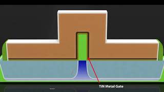
Yes! The FinFET uses a 3D structure that greatly enhances control over the electrostatics.
Features of FinFET Technology
🔒 Unlock Audio Lesson
Sign up and enroll to listen to this audio lesson
FinFETs have become a significant advancement in technology. Can anyone recall one key advantage?
Better control over leakage?
Correct! They offer lower leakage currents. Another advantage is they can drive higher current due to their effective channel width. What else?
They use less power!
Exactly! FinFETs can operate at lower supply voltages, leading to improved power efficiency.
Future Trends: GAA FET
🔒 Unlock Audio Lesson
Sign up and enroll to listen to this audio lesson
After FinFETs, there's also the GAA FET. Can anyone guess what 'Gate-All-Around' means?
Does it mean that the gate surrounds the channel?
Right! This design improves control over the channel even further. It's an exciting next step for transistor technology!
I can see why advancements are necessary. Technology keeps scaling down!
Exactly! Keeping up with these advancements is essential for the future of electronics.
Introduction & Overview
Read summaries of the section's main ideas at different levels of detail.
Quick Overview
Standard
The section examines the transition from planar MOSFETs to FinFETs, detailing various generations of MOSFET technology, the limitations of planar MOSFETs beyond 22nm, and the emergence of FinFETs as a solution to these challenges, offering improved performance, efficiency, and scalability.
Detailed
Evolution: From MOSFETs to FinFETs
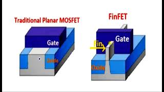
As the semiconductor industry faced challenges in continuing Moore's Law, traditional planar MOSFETs became less viable beyond 22 nm technology nodes. This led to the development of Fin Field Effect Transistors (FinFETs), which are characterized by a three-dimensional fin-shaped channel that enhances electrostatic control.
Generational Advancements
- Planar MOSFETs: Traditional two-dimensional structure with limited performance at smaller scales.
- Strained MOSFETs: Employed strained silicon to enhance carrier mobility.
- High-κ/Metal Gate (HKMG): Introduced a material substitution to reduce gate leakage.
- FinFETs: Implemented a 3D fin structure providing superior gate control and performance.
- GAA FET: Future technology for even greater control than FinFETs, showcasing the ongoing evolution.
Limitations of Traditional MOSFETs
The failure of planar MOSFET technology is due to severe short-channel effects, increased leakage current, and power consumption at scales smaller than 22 nm. This necessitated the development of new architectures.
Significance
Understanding the transition to FinFETs is crucial for comprehending modern semiconductor technology and its applications in advanced processors and low-power devices.
Youtube Videos


Audio Book
Dive deep into the subject with an immersive audiobook experience.
Generation Features
Chapter 1 of 2
🔒 Unlock Audio Chapter
Sign up and enroll to access the full audio experience
Chapter Content
Generation Features
- Planar MOSFET: Traditional 2D structure with gate over a flat channel
- Strained MOSFETs: Enhanced mobility using strained silicon
- High-κ/Metal Gate (HKMG): Replaced silicon dioxide gate to reduce gate leakage
- FinFET: Introduced 3D fin-shaped channel for better gate control
- GAA FET (future): Gate-All-Around FET with even better control than FinFETs
Detailed Explanation
This chunk outlines the evolution of transistor technology from traditional MOSFETs to FinFETs and beyond. Each generation of transistors has introduced improvements to address the limitations of previous designs. The traditional planar MOSFET features a flat channel, while the strained MOSFET enhances mobility through material modifications. High-κ/Metal Gate technology replaces the conventional silicon dioxide gate to prevent leakage. The FinFET introduces a new 3D fin-shaped structure that significantly improves gate control over the channel. Finally, the GAA FET represents the future of transistor design by providing even more superior control of the channel's electrostatics.
Examples & Analogies
Think of the evolution of smartphone cameras. The first smartphone cameras were basic and flat (like the planar MOSFET), then manufacturers started adding features like enhanced sensors (strained MOSFETs), and now we have multi-lens systems with improved functionality (FinFETs and GAA FETs) that can take stunning pictures under various conditions.
Why Planar MOSFETs Failed Beyond 22nm
Chapter 2 of 2
🔒 Unlock Audio Chapter
Sign up and enroll to access the full audio experience
Chapter Content
Why Planar MOSFETs Failed Beyond 22nm:
- Severe short-channel effects (SCEs)
- Leakage current due to thin gate oxide
- Poor electrostatic control over the channel
- Increased power consumption
Detailed Explanation
This chunk discusses the limitations of planar MOSFETs as they reached miniaturization below 22nm. The severe short-channel effects (SCEs) occur when the channel length becomes very short, causing the transistor to operate unpredictably. Additionally, a thinner gate oxide layer results in higher leakage currents, where electrons seep through unintentionally, reducing efficiency. The electrostatic control becomes poor, meaning the gate struggles to regulate the channel effectively. Lastly, the miniaturization increases power consumption, which is counterproductive for devices that aim to be energy efficient.
Examples & Analogies
Imagine trying to control water flow through a very thin straw. As the straw gets shorter and shorter, it becomes harder to control the flow, and small leaks start to occur. Just like that straw, planar MOSFETs struggle to manage electrical currents efficiently as they shrink beyond certain sizes.
Key Concepts
-
Planar MOSFET: Traditional 2D structure limited in performance at small scales.
-
Strained MOSFET: Enhanced mobility using strained silicon.
-
FinFET: A 3D transistor design overcoming limitations of 2D MOSFETs.
-
GAA FET: Future technology providing even better control than FinFETs.
Examples & Applications
The transition from 2D planar MOSFETs to 3D FinFETs exemplifies how technology must adapt to maintain efficiency at smaller scales.
The application of FinFETs in modern CPUs showcases their advantages in controlling leakage and enhancing drive current.
Memory Aids
Interactive tools to help you remember key concepts
Rhymes
When MOSFETs scaled, they began to fail, FinFETs rose with a new detail.
Stories
Imagine planar transistors trying to fit into a tiny box. They struggled until the FinFET came, bringing extra sides, it was no longer stuck!
Memory Tools
To remember the benefits of FinFET: 'F.E.L.P.' - for 'Faster', 'Efficient', 'Lower leakage', 'Power effective'.
Acronyms
Remember 'SLEP'
'Short-channel effects'
'Leakage'
'Electrostatic control'
and 'Power consumption' to recall why MOSFETs failed.
Flash Cards
Glossary
- MOSFET
Metal-Oxide-Semiconductor Field-Effect Transistor; a type of transistor used for switching and amplifying electronic signals.
- FinFET
Fin Field Effect Transistor; a type of non-planar, 3D transistor used to improve electrostatic control and performance over traditional MOSFETs.
- Shortchannel effects (SCEs)
Phenomena occurring in transistors when their physical dimensions shrink, leading to loss of control over the current flow.
- Leakage current
Unwanted flow of current that occurs when a semiconductor device is in an off state.
- Power consumption
The amount of power used by a device during operation, important for efficiency in electronics.
Reference links
Supplementary resources to enhance your learning experience.