
Introduction to FinFET Technology
Interactive Audio Lesson
Listen to a student-teacher conversation explaining the topic in a relatable way.
Advantages of FinFET Technology
🔒 Unlock Audio Lesson
Sign up and enroll to listen to this audio lesson

Now, let’s discuss the advantages of using FinFET technology. Who can tell me why power efficiency is better with FinFETs?

Because they can operate at lower supply voltages!
Correct! Lower voltage operation helps reduce power consumption. Remember 'Performance per Watt' as a key benefit. How about electrostatic control?

The wrapping structure lowers drain-induced barrier lowering?
Exactly! This enhances immunity against short-channel effects. FinFETs allow improved scalability as well. Can anyone tell me what the minimum node size FinFETs are suited for?

Less than 14nm, right?
Spot on! They’re indeed suitable for technology nodes below 14nm. In summary, FinFETs offer better electrostatic control, lower leakage currents, and greater scalability compared to traditional planar MOSFETs.
Introduction & Overview
Read summaries of the section's main ideas at different levels of detail.
Quick Overview
Standard
As traditional planar MOSFETs reached their scaling limits, FinFETs emerged as a solution, offering improved electrostatic control, lower leakage currents, and higher drive currents. This section explores the evolution from MOSFETs to FinFETs, their structure, advantages, challenges, applications, and comparisons with planar MOSFETs.
Detailed
Introduction to FinFET Technology
Overview
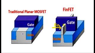
As conventional planar MOSFETs approach their performance limits, Fin Field Effect Transistors (FinFETs) have been developed to sustain Moore's Law, enabling advancements in semiconductor technology. FinFETs are 3D transistors characterized by their fin-like structures that enhance control over the channel, particularly at technology nodes of 22 nm or less.
Evolution from MOSFETs to FinFETs
The transition from traditional MOSFETs to FinFETs is a response to the challenges posed by scaling down devices. While planar MOSFETs are limited by short-channel effects, leakage currents, poor electrostatic control, and increased power consumption, FinFETs introduce a vertical channel structure that wraps the gate around the channel for better control.
Structure and Operation
A FinFET features a fin structure that rises from the substrate, allowing the gate to effectively control the channel on three sides. This enables reduced leakage current and improved drive current, thanks to the use of high-κ materials.
Types of FinFETs
Different types of FinFETs include Double-Gate and Tri-Gate designs, which offer varying degrees of control and performance advantages.
Advantages and Challenges
FinFET technology presents several benefits such as improved electrostatic control, lower power consumption, and scalability for sub-14 nm nodes. However, it also comes with complexities in fabrication and design, alongside increased costs.
Applications
FinFETs are widely used in microprocessors, low-power devices, and high-performance computing applications, including modern chips produced by leading semiconductor manufacturers.
Comparison with Planar MOSFETs
Comparing FinFETs with traditional planar MOSFETs reveals significant advantages in control, leakage current management, and overall efficiency, highlighting their importance in the future of semiconductor technology.
Youtube Videos


Audio Book
Dive deep into the subject with an immersive audiobook experience.
Introduction to FinFETs
Chapter 1 of 4
🔒 Unlock Audio Chapter
Sign up and enroll to access the full audio experience
Chapter Content
As traditional planar MOSFETs reached their scaling limits, device engineers developed Fin Field Effect Transistors (FinFETs) to continue Moore’s Law.
- FinFETs are a type of non-planar, 3D transistor used in advanced CMOS technology nodes (≤22 nm).
- They offer better control of short-channel effects, lower leakage currents, and higher drive current.
Detailed Explanation
This chunk introduces FinFETs, a type of transistor designed to overcome the challenges faced by traditional planar MOSFETs, especially as electronic components have to become smaller and more efficient. 'Moore’s Law' suggests that the number of transistors on a microchip doubles approximately every two years, which means constant innovation is necessary in semiconductor technology. FinFETs, being three-dimensional and non-planar, significantly improve control over short-channel effects, which occur when transistors shrink in size—leading to problems such as increased leakage currents and reduced performance. By providing a 3D structure, FinFETs allow for better performance at smaller sizes, specifically in technology nodes of 22 nanometers and below.
Examples & Analogies
Think of traditional MOSFETs as flat, two-dimensional cars on a road that can only go so fast before they reach their limits. Now, imagine FinFETs as innovative flying cars that can navigate in three-dimensional space, overcoming obstacles and utilizing their design to achieve higher speeds and efficiency. Just as flying cars can go beyond traditional vehicles' limitations, FinFETs allow semiconductor technology to continue advancing.
Why Traditional MOSFETs Failed
Chapter 2 of 4
🔒 Unlock Audio Chapter
Sign up and enroll to access the full audio experience
Chapter Content
- Severe short-channel effects (SCEs)
- Leakage current due to thin gate oxide
- Poor electrostatic control over the channel
- Increased power consumption
Detailed Explanation
This chunk discusses the reasons traditional planar MOSFETs became inadequate for technology nodes below 22 nm. As manufacturers attempted to shrink MOSFETs further, they encountered significant issues known as short-channel effects. These effects lead to degradation in performance as the control over the channel becomes weaker, resulting in higher leakage currents—unwanted currents that drain power and can cause the circuits to behave erratically. The thin gate oxide needed for smaller devices also exacerbates these problems, causing more leakage and making electrostatic control more difficult, ultimately leading to higher power consumption requirements.
Examples & Analogies
Imagine trying to control a very small water flow using a tiny pipe. If the pipe is too thin or short, the water starts spraying everywhere instead of flowing smoothly, just like how MOSFETs struggle to control electricity as they shrink. As the pipe gets smaller, maintaining control becomes harder, leading to messy leaks, which is essentially what happens with traditional MOSFETs at smaller nodes.
FinFET Structure
Chapter 3 of 4
🔒 Unlock Audio Chapter
Sign up and enroll to access the full audio experience
Chapter Content
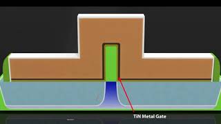
- FinFET has a fin-like vertical channel rising from the substrate.
- Gate wraps around three sides of the fin, improving control over the channel.
Element Description: - Fin: Thin strip of silicon forms the channel
- Gate: Covers the top and sides of the fin
- Source/Drain: Located at the ends of the fin
- Gate: Often made of high-κ material for reduced dielectric leakage.
Detailed Explanation
Here, we delve into the structure of FinFETs, which is fundamentally different from that of traditional MOSFETs. The 'fin' design allows for a vertical channel that significantly enhances the interaction between the gate and the channel. Since the gate surrounds three sides of this fin-shaped channel, it provides much better electrostatic control, helping to mitigate the issues associated with short-channel effects. Additionally, the materials used, such as high-κ materials, minimize leakage, ensuring more effective performance.
Examples & Analogies
Consider a fin as a tall, narrow building surrounded by protective walls on three sides. By being enclosed, those walls (the gate) can manage the environment around the building much better, just as the gate's control over the fin improves overall transistor performance. This is akin to how smart building designs optimize energy by maintaining a comfortable interior while reducing waste.
Types of FinFETs
Chapter 4 of 4
🔒 Unlock Audio Chapter
Sign up and enroll to access the full audio experience
Chapter Content
- Double-Gate: Gate on two sides of the fin
- Tri-Gate: Gate on both sides and the top of the fin
- Multi-Gate: General term for more than one gate on a channel
Detailed Explanation
This chunk outlines the different types of FinFETs based on the number and positioning of the gates. The Double-Gate design has gates on two sides of the fin, providing improved control over its electrical characteristics. Tri-Gate designs enhance this further by adding a gate on top, thus offering even better control and performance. The term Multi-Gate broadly encapsulates any design that includes multiple gates, allowing for flexibility in device design for specific applications.
Examples & Analogies
Imagine different styles of protective barriers around a garden. A single fence offers basic protection, while a double fence (like the Double-Gate FinFET) makes it harder for pests to enter. Now, visualize adding a roof over the garden (the Tri-Gate), which provides complete coverage and protection, similar to how additional gates enhance the control provided by FinFETs.