
Challenges of FinFET Technology
Interactive Audio Lesson
Listen to a student-teacher conversation explaining the topic in a relatable way.
Complex Fabrication
🔒 Unlock Audio Lesson
Sign up and enroll to listen to this audio lesson

Today, we're talking about one of the main challenges of FinFET technology: complex fabrication. FinFETs require advanced 3D patterning and etching techniques. Can anyone tell me why these methods might increase variability?

I think it's because making fins in 3D is harder than just etching a flat surface.
Exactly! The precision needed in the 3D dimensions can cause variations in fin characteristics which affect device performance. This can lead to variations in electrical properties between transistors.

So, a small mistake can lead to significant problems?
Yes, even small fabrication errors can have a big impact. That's why controlling the fabrication process is so critical for FinFETs.
Let's remember this with the mnemonic: '3D FINS,' which stands for 'Three-Dimensional Fin Requires Intense Nano-scale Precision.' Keep that in mind as we move on!

Could errors here affect production yield too?
Absolutely! Increased variability can lead to lower yields, complicating the overall production process.
Increased Cost
🔒 Unlock Audio Lesson
Sign up and enroll to listen to this audio lesson

Now, let's discuss cost implications. Why do you think FinFET technology is more expensive?
Is it because it needs more advanced lithography?
Yes, that's one reason! The need for advanced lithography is greater due to the complexity of 3D structures. More intricate processes mean higher costs for manufacturers.

Does that mean the end products are more expensive too?
Correct! The increased production costs are likely to be passed on to consumers, making devices using FinFETs more expensive.
Remember: 'COST,' which stands for 'Complexity Overheads Stemming from Technology.' Keep that in mind when we discuss market adaptations next!
Design Complexity
🔒 Unlock Audio Lesson
Sign up and enroll to listen to this audio lesson
Another significant challenge is design complexity. Why do you think designers need new Electronic Design Automation tools for FinFETs?
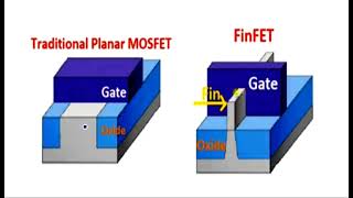
Because FinFETs are different from planar MOSFETs, right? They have that 3D structure!
Exactly! The unique design aspects, such as the quantized width of fins, necessitate specialized design tools that can handle these variations.
So old tools won’t work well?
Correct! Legacy EDA tools may struggle with the complexities associated with FinFET designs.
Let's remember this complexity with the acronym 'E.D.A.: Every Design and Automation requires accuracy.'
Heat Dissipation
🔒 Unlock Audio Lesson
Sign up and enroll to listen to this audio lesson
Lastly, we have heat dissipation challenges. Can someone elaborate on why thermal issues are more prevalent with FinFETs?
Is it because they are more densely packed together?
That's right! The 3D structure and higher density can lead to difficulty in managing the heat generated.
Could this impact performance too?
Absolutely! Poor heat dissipation can lead to increased operating temperature and potentially affect the reliability of the device.
To remember this, think 'HEAT' - 'High Efficiency Affects Temperature'.
Introduction & Overview
Read summaries of the section's main ideas at different levels of detail.
Quick Overview
Standard
The challenges of FinFET technology encompass complex fabrication processes, increased costs, design complexities, and heat dissipation issues, which pose significant hurdles in advancement and implementation. Understanding these challenges is crucial for improving existing semiconductor technologies.
Detailed
Challenges of FinFET Technology
The adoption of FinFET technology comes with various challenges that need to be addressed to fully leverage its advantages. These challenges include:
1. Complex Fabrication
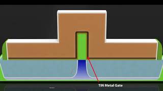
The 3D structure of FinFETs requires highly precise fabrication techniques, such as advanced 3D patterning and etching methods. This complexity can lead to higher variability in fin dimensions, which impacts device performance.
2. Increased Cost
Implementing FinFET technology demands more advanced lithography and processing steps, resulting in higher manufacturing costs compared to traditional planar MOSFETs.
3. Design Complexity
The intricate designs necessitate the development of new Electronic Design Automation (EDA) tools and models to effectively work with FinFET structures. Moreover, the quantized width of fins introduces limitations, making design further complicated.
4. Heat Dissipation
The denser packing of FinFETs can lead to severe thermal issues. As transistors become smaller and more densely packed, the ability to manage heat becomes increasingly difficult, raising concerns about performance and reliability.
Understanding these challenges is essential for engineers and designers as they work towards innovating and improving semiconductor technologies, particularly as we continue to push the limits of Moore's Law.
Youtube Videos


Audio Book
Dive deep into the subject with an immersive audiobook experience.
Complex Fabrication
Chapter 1 of 4
🔒 Unlock Audio Chapter
Sign up and enroll to access the full audio experience
Chapter Content
❌ Complex Fabrication
● Requires precise 3D patterning and etching
● Higher variability due to fin dimensions
Detailed Explanation
FinFET technology involves complex manufacturing processes. Unlike traditional transistors that are mostly planar, FinFETs have a three-dimensional structure that demands careful and precise patterning during fabrication. This includes etching fins to the exact size and placing them with high accuracy. Because of their intricate design, even small variations in the dimensions of the fins can lead to significant differences in performance, which can make the manufacturing process less predictable and more challenging.
Examples & Analogies
Think of creating a sculpture from clay. If you try to carve a delicate design with very fine details, even a slight mistake can ruin the whole sculpture. In the same way, the nuances in shaping FinFETs can lead to imperfections that affect how they work.
Increased Cost
Chapter 2 of 4
🔒 Unlock Audio Chapter
Sign up and enroll to access the full audio experience
Chapter Content
❌ Increased Cost
● More expensive lithography and process steps
Detailed Explanation
The advanced processes required to fabricate FinFETs are more expensive compared to traditional planar MOSFETs. This is largely due to the need for new lithography techniques and the additional steps included in the manufacturing process. As a result, the overall cost of production increases, which can impact the price of the final products that use FinFET technology.
Examples & Analogies
Imagine cooking a gourmet meal that requires specialized ingredients and sophisticated cooking techniques. The overall cost of making that meal will be much higher than if you were just preparing a simple sandwich. Similarly, using advanced FinFET technology means incurring higher costs to produce chips.
Design Complexity
Chapter 3 of 4
🔒 Unlock Audio Chapter
Sign up and enroll to access the full audio experience
Chapter Content
❌ Design Complexity
● Need for new EDA tools and models
● Limited by quantized width (discrete number of fins)
Detailed Explanation
With FinFETs, circuit designers face new challenges that necessitate the use of updated electronic design automation (EDA) tools and models. These tools are needed to effectively manage and simulate the more intricate three-dimensional designs of FinFET transistors. Moreover, the distinct structure of FinFETs means they can only be designed with a specific number of fins, which complicates the design process since it is not a simple continuous variable like traditional transistors.
Examples & Analogies
Consider how creating a piece of modern art can require new techniques and tools that differ from traditional painting. Just as artists may need new brushes and mediums for innovative artworks, engineers must adapt and develop new tools to design with FinFET technology.
Heat Dissipation
Chapter 4 of 4
🔒 Unlock Audio Chapter
Sign up and enroll to access the full audio experience
Chapter Content
❌ Heat Dissipation
● Denser packing leads to thermal issues
Detailed Explanation
FinFETs facilitate more compact designs, allowing for more transistors to be packed into smaller areas on a chip. However, this density can lead to significant heat buildup during device operation. Managing this heat is crucial, as excessive heat can affect performance and reliability in electronic devices, making thermal management a vital concern for engineers designing with FinFETs.
Examples & Analogies
Think of a crowded subway train; as more people pack into the car, it tends to get hotter due to increased body heat and limited ventilation. Similarly, as more FinFETs are packed together on a chip, managing the heat they produce becomes increasingly challenging.
Key Concepts
-
Complex Fabrication: FinFETs require precise 3D patterning which increases variability.
-
Increased Cost: Advanced manufacturing techniques lead to higher expenses.
-
Design Complexity: Requires new EDA tools for complex designs.
-
Heat Dissipation: Denser layouts lead to thermal management challenges.
Examples & Applications
The use of FinFETs in the latest generation of Intel processors demonstrates complex fabrication requirements due to their advanced 3D structure.
Smartphones using FinFET technology can suffer from thermal throttling during high performance due to inefficient heat dissipation.
Memory Aids
Interactive tools to help you remember key concepts
Rhymes
FinFET transistors are the best, but heat and cost can put them to the test.
Stories
Once upon a time in the land of silicon, FinFETs emerged with their 3D structures. However, they faced trolls of complexity, cost, and heat, guarding the path to technological advancement.
Memory Tools
Remember C.D.H. for understanding FinFET challenges: Complexity, Design, Heat.
Acronyms
HEAT
High Efficiency Affects Temperature.
Flash Cards
Glossary
- FinFET
A type of non-planar, three-dimensional transistor used in advanced CMOS technology.
- Fabrication
The process of manufacturing semiconductor devices.
- EDA (Electronic Design Automation)
Software tools used for designing electronic systems.
- Heat Dissipation
The process of removing excess heat from a semiconductor device.
- Quantized Width
The discrete width of fins in FinFETs that affects their design.
Reference links
Supplementary resources to enhance your learning experience.