
Summary of Key Concepts
Interactive Audio Lesson
Listen to a student-teacher conversation explaining the topic in a relatable way.
Introduction to FinFETs
🔒 Unlock Audio Lesson
Sign up and enroll to listen to this audio lesson

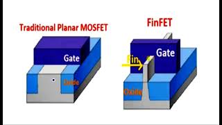
Today, we’re talking about FinFETs, a key technology in modern semiconductors. Can anyone tell me what sets FinFETs apart from traditional planar MOSFETs?

I think FinFETs are 3D transistors that help with better control over short-channel effects.
Exactly! They operate at nodes below 22nm and provide superior electrostatic control. This is crucial for performance. Remember, 3D stands for 'three dimensions' meaning they stack a lot more functionality into a smaller footprint.

What do you mean by controlling short-channel effects?
Good question! Short-channel effects occur when the channel length is short, which can cause unwanted behaviors in the transistor. FinFETs minimize these effects by allowing the gate to surround the channel more effectively.

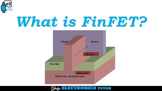
So, the gate wraps around the fin?
Exactly! This wraps around three sides, enhancing control. That’s a fundamental concept about FinFETs we should remember.

What are some of the advantages then?
Great follow-up! FinFETs reduce leakage currents, enhance drive current, and offer better scalability—making them suitable for lower power applications. Overall, these factors contribute to making FinFETs the industry standard.
To recap, FinFETs are 3D transistors that enable better control and performance at small nodes, perfect for the advancing demands in technology.
Challenges of FinFETs
🔒 Unlock Audio Lesson
Sign up and enroll to listen to this audio lesson

While we've covered the advantages of FinFETs, let’s discuss the challenges involved in their fabrication and design. What do you think these might be?
I think it might be more complex due to the 3D structure.
Correct! The fabrication process indeed involves more intricate steps like 3D patterning which can lead to variability. This increases the cost and effort needed compared to planar MOSFETs.
So, does that mean they are only used in high-end applications?
Not necessarily. Although FinFETs are more expensive and complex, they're also essential for modern devices that demand high performance, like processors and GPUs. The trade-off is necessary for advanced technology.
What about heat dissipation? Is that a problem too?
Absolutely! As more fins are packed into a smaller area, heat dissipation becomes critical. This is an ongoing challenge engineers need to address.
To summarize, while FinFETs provide significant benefits, their complexity in design and fabrication, as well as thermal management, are key challenges we must be aware of.
Introduction & Overview
Read summaries of the section's main ideas at different levels of detail.
Quick Overview
Standard
FinFET technology represents a significant evolution in transistor design, providing enhanced gate control, lower leakage currents, and improved scalability compared to planar MOSFETs. Despite their manufacturing complexities, FinFETs have become an industry standard due to their advantages in performance and power efficiency.
Detailed
Summary of Key Concepts
Fin Field Effect Transistors, or FinFETs, have emerged as a solution to the limitations faced by traditional planar MOSFETs, especially at technology nodes of 22nm and below. Unlike conventional 2D devices, FinFETs utilize a three-dimensional structure that enhances control over the channel, significantly mitigating short-channel effects (SCE). With their superior performance characteristics—including reduced leakage currents and increased scalability—FinFETs are increasingly adopted across the semiconductor industry.
However, these advancements come with certain challenges. The fabrication of FinFETs is more complex and costly compared to their planar counterparts, requiring advanced processes and new design tools. Despite these hurdles, the performance benefits of FinFET technology have established it as the preferred choice for modern high-performance applications, marking a pivotal shift in semiconductor technology.
Youtube Videos

Audio Book
Dive deep into the subject with an immersive audiobook experience.
Introduction to FinFETs
Chapter 1 of 3
🔒 Unlock Audio Chapter
Sign up and enroll to access the full audio experience
Chapter Content
● FinFETs are 3D, multi-gate transistors designed to overcome the limitations of planar MOSFETs at sub-22nm nodes.
Detailed Explanation
FinFETs are a new type of transistor that are designed in three dimensions, allowing for better performance than traditional planar MOSFETs, which are designed in two dimensions. The 'multi-gate' aspect means that they have multiple gates that control the flow of electrical current, making them more effective in smaller nodes (like those below 22 nanometers). Essentially, the geometry of the FinFET allows it to control current more effectively as chip sizes shrink.
Examples & Analogies
Think of a FinFET like a multi-lane highway compared to a traditional road. A multi-lane highway allows more cars (current) to travel simultaneously and more efficiently than a single-lane road, especially when there is a lot of traffic (like in very small chip designs).
Key Benefits of FinFETs
Chapter 2 of 3
🔒 Unlock Audio Chapter
Sign up and enroll to access the full audio experience
Chapter Content
● They provide superior gate control, reduced leakage, and better scalability, but come with fabrication and design complexities.
Detailed Explanation
One of the main advantages of FinFETs is that they offer much better control over the flow of electricity (superior gate control) compared to traditional transistors. This leads to reduced leakage currents, which can waste energy. Additionally, FinFETs are scalable, meaning that as technology advances, they can be made smaller and more efficient without losing effectiveness. However, developing these transistors is more complicated due to the intricate fabrication processes involved and the new designs that engineers must create.
Examples & Analogies
Imagine trying to maintain a garden. If you have more tools and better techniques (FinFET technology), you can grow healthier plants (better performance) with less water wasted (reduced leakage). However, learning new gardening techniques and handling more specialized tools can be more challenging and complex.
The Industry Standard
Chapter 3 of 3
🔒 Unlock Audio Chapter
Sign up and enroll to access the full audio experience
Chapter Content
● FinFETs have become the industry standard for advanced CMOS technologies.
Detailed Explanation
As the demands for faster and more efficient electronics grow, FinFET technology has been widely adopted across the semiconductor industry. Its advantages in performance, efficiency, and ability to keep up with Moore's Law—where the number of transistors on a chip doubles approximately every two years—have made FinFETs the go-to choice for manufacturers of advanced chips.
Examples & Analogies
Consider how smartphones have rapidly evolved. Just like how sleek new smartphone designs and faster processors become the standard as technology grows, FinFETs have set a new benchmark in chip design, making them essential for developing high-performance devices.
Key Concepts
-
FinFET: A revolutionary 3D transistor design enhancing gate control and scalability.
-
Electrostatic Control: Improved management of short-channel effects and leakage currents.
-
Scalability: The ability of FinFETs to be effectively used at technology nodes below 22nm.
Examples & Applications
FinFETs are commonly used in modern processors like Intel's Core i7, where reduced leakage current and increased drive capabilities are necessary.
Advancements in smartphone technology utilize FinFETs to maintain battery life while enhancing performance.
Memory Aids
Interactive tools to help you remember key concepts
Rhymes
FinFET technology takes flight, reducing leakage with all its might.
Stories
Imagine a tiny fin in a bustling lake. It helps control water flows better than flat surfaces; this fin represents how FinFET transistors improve control in electronics.
Memory Tools
For FinFET: 'Fighting Inadequate Nodes, Faster Efficient Transistors' to remember its role.
Acronyms
FINS - 'Fin in New Semiconductor' to emphasize the innovation.
Flash Cards
Glossary
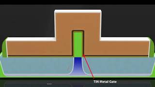
- FinFET
A 3D transistor structure that improves electrostatic control by allowing the gate to wrap around the channel.
- ShortChannel Effects (SCE)
Unwanted behaviors occurring in transistors as the channel length decreases, negatively affecting performance.
- Leakage Current
Unintended current that flows through a device when it is off, leading to power loss.
- CMOS
Complementary metal-oxide-semiconductor technology used in electronic circuits.
- Drive Current
The current that a transistor can provide to drive a load, important for performance.
Reference links
Supplementary resources to enhance your learning experience.