
FinFET Structure and Operation
Interactive Audio Lesson
Listen to a student-teacher conversation explaining the topic in a relatable way.
Introduction to FinFET Structure
🔒 Unlock Audio Lesson
Sign up and enroll to listen to this audio lesson

Today, we’re diving into the world of FinFETs. Can anyone tell me what a FinFET is?

Is it a type of transistor?
Correct! A FinFET is a transistor design that allows better control and efficiency. The key feature is its vertical fin-shaped channel. Why do you think that matters?

Maybe it helps reduce leakage current?
Exactly! Since the gate can wrap around the fin, it improves electrostatic control, which is critical for reducing leakage. Remember the acronym *GFS* for Gate, Fin, Source – it helps you remember the main components!

So, the fin is what conducts the current?
Yes, indeed! And understanding these components helps us appreciate why FinFETs are preferred in advanced CMOS technology.
Operational Principles of FinFETs
🔒 Unlock Audio Lesson
Sign up and enroll to listen to this audio lesson

Let’s discuss how FinFETs operate. What makes them better than traditional planar MOSFETs?

I think it has something to do with short-channel effects.
Right! The 3D design significantly alleviates short-channel effects, which is crucial as we move to smaller technology nodes. Can anyone explain what leakage current is?
It's unwanted current that occurs when the device is supposed to be off.
Exactly! FinFETs have a lower leakage current due to the way the gate surrounds the channel. Always think of *GDFS* (Gate, Drain, Fin, Source) when recalling their layout.
And that helps them carry more current too?
Yes! The fin structure allows for a larger effective channel width, improving drive current and speed.
Comparison with Planar MOSFETs
🔒 Unlock Audio Lesson
Sign up and enroll to listen to this audio lesson
Let's compare FinFETs with planar MOSFETs. What do you think are the main differences?
I know FinFETs have better control over short-channel effects.
Correct! In fact, the planar structure struggles with these effects as features shrink. Can anyone name a disadvantage of FinFETs?
They might be more complex to fabricate?
Yes! Fabrication complexity is a key challenge. Remember: *SPL* – Short-channel effects, Power consumption, and Leakage current are key points when comparing these technologies.
So, FinFETs are preferable for advanced technologies?
Indeed, especially for nodes below 22 nm. They represent the future of transistor technology in high-performance applications.
Introduction & Overview
Read summaries of the section's main ideas at different levels of detail.
Quick Overview
Standard
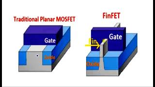
The FinFET structure features a vertical, fin-like channel that significantly enhances gate control by allowing the gate to wrap around three sides of the fin. This design reduces leakage current and improves drive current capability, making FinFETs the preferred choice for advanced CMOS technology nodes.
Detailed
FinFET Structure and Operation
FinFETs, or Fin Field Effect Transistors, exemplify a leap in transistor design, transitioning from the traditional planar MOSFETs to a three-dimensional structure that vastly improves electrical performance.
Key Components:
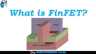
- Fin: The thin vertical strip of silicon that forms the channel through which current flows.
- Gate: The control element that wraps around three sides of the fin, allowing enhanced electrostatic control over the channel.
- Source/Drain: These are located at either end of the fin, completing the path for current.
Advantages of FinFETs Over Planar MOSFETs:
By implementing a design where the gate surrounds the fin, FinFETs gain better control of short-channel effects (SCEs), leading to reduced leakage currents and improved drive current capacity. This 3D architecture allows for the carrying of more current than traditional planar FETs, making FinFETs ideal for smaller technology nodes (≤22 nm), thus continuing the trend of Moore's Law.
Youtube Videos

Audio Book
Dive deep into the subject with an immersive audiobook experience.
FinFET Channel Structure
Chapter 1 of 4
🔒 Unlock Audio Chapter
Sign up and enroll to access the full audio experience
Chapter Content
● FinFET has a fin-like vertical channel rising from the substrate.
Detailed Explanation
A FinFET is designed with a unique vertical channel that looks like a fin standing upright from the surface of the substrate (the underlying material). This fin shape allows the transistor to have a better configuration for controlling the current that flows through it compared to traditional planar transistors. The fin's height provides a three-dimensional effect, which is crucial for the performance of the device, especially at smaller scales.
Examples & Analogies
Imagine a traditional flat bridge (planar transistor) versus a multi-layered, tall tower bridge (FinFET). The tower can better manage traffic flow because it's higher and has more levels of entry and exit points, similar to how the vertical structure of a FinFET enhances control of electrical currents.
Gate Design
Chapter 2 of 4
🔒 Unlock Audio Chapter
Sign up and enroll to access the full audio experience
Chapter Content
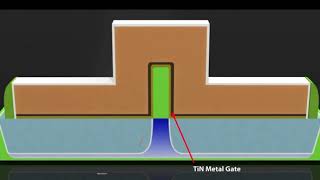
● Gate wraps around three sides of the fin, improving control over the channel.
Detailed Explanation
In a FinFET, the gate—the component responsible for controlling the flow of current—envelops the top and sides of the fin. This wrapping design allows the gate to exert control over the channel from multiple angles rather than just one side like in traditional planar designs. This improved control leads to better efficiency in switching on and off the current, reducing unwanted leakage and enhancing the performance of the semiconductor device.
Examples & Analogies
Think of a person trying to control the flow of a river. If they only stand on one side of the river (like the traditional gate), they have limited control. However, if they can walk around the river's edges and even stand on a bridge above (like the FinFET's gate), they can better manage the water flow from multiple viewpoints, which leads to a calmer and more predictable current.
Fin and Gate Materials
Chapter 3 of 4
🔒 Unlock Audio Chapter
Sign up and enroll to access the full audio experience
Chapter Content
● Element Description: Fin: Thin strip of silicon forms the channel; Gate: Covers the top and sides of the fin; Source/Drain: Located at the ends of the fin; Gate: Often made of high-κ material for reduced dielectric leakage.
Detailed Explanation
The 'fin' of a FinFET is made from a thin strip of silicon which serves as the channel where charge carriers (electrons or holes) flow. The gate material, commonly a high-κ (high-kappa) dielectric, is used to improve efficiency by minimizing gate leakage (unwanted current flow through the gate). The source and drain are contact points where current enters and exits the fin, respectively. Utilizing high-κ materials enhances the transistor's ability to control the channel while maintaining lower power loss.
Examples & Analogies
Think of the finlike channel as a water pipe (the fin), with the gate as a highly efficient valve (the gate) that can regulate water flow (current), and the ends of the pipe (source and drain) are where the water enters and exits. Using a well-designed valve (high-κ material) ensures less water leaks out when it’s meant to be shut, allowing for a smoother operation overall.
Current Carrying Capacity
Chapter 4 of 4
🔒 Unlock Audio Chapter
Sign up and enroll to access the full audio experience
Chapter Content
Depending on the number of fins, FinFETs can carry more current than planar FETs.
Detailed Explanation
One of the advantages of FinFETs is that by utilizing multiple fins (i.e., stacking or placing several fins in parallel), these transistors can handle significantly more current compared to their planar counterparts. This capability is crucial for modern applications that demand high performance and efficiency, especially as circuitry becomes increasingly compact and complex. The more fins you have, the greater the effective channel width, allowing for higher current flow.
Examples & Analogies
Imagine a multi-lane highway (multiple fins) as opposed to a single-lane country road (planar FET). The multi-lane highway can accommodate many more cars (current), enabling a more efficient flow of traffic, which parallels how multiple fins within a FinFET design enhance current-carrying capacity.
Key Concepts
-
FinFET Structure: A three-dimensional design with a vertical fin-shaped channel.
-
Gate Control: Enhanced by wrapping around three sides of the fin.
-
Advantages Over MOSFETs: Better performance in terms of leakage current and short-channel effects.
Examples & Applications
The use of FinFETs in Intel's 10nm process technology demonstrates the scalability and performance of 3D transistors.
In smartphones, FinFET technology enables better battery life and faster processing speeds due to reduced leakage currents.
Memory Aids
Interactive tools to help you remember key concepts
Rhymes
A Fin comes up from the silicon flat, the gate wraps around, just like that!
Stories
Imagine a tall building (the fin) with balconies (the gate) surrounding it, ensuring no one falls off – that’s how FinFETs work to protect against leakage and short channel effects!
Memory Tools
Remember 'GFS' for FinFET: Gate, Fin, Source – the order of components!
Acronyms
Use the acronym 'GDFS' to remember Gate, Drain, Fin, Source for FinFET structures.
Flash Cards
Glossary
- Fin
A thin strip of silicon that forms the channel in a FinFET.
- Gate
The control element that wraps around the fin, allowing better control over the channel.
- Source/Drain
Components located at the ends of the fin, allowing current to flow through the device.
- Shortchannel effects (SCEs)
Issues arising in MOSFETs as devices shrink, affecting performance due to lack of electrostatic control.
- Leakage current
Unwanted current that flows through a device when it should be off, affecting power efficiency.
Reference links
Supplementary resources to enhance your learning experience.