
FPGA Design Flow
Interactive Audio Lesson
Listen to a student-teacher conversation explaining the topic in a relatable way.
Specification and Requirements Definition
🔒 Unlock Audio Lesson
Sign up and enroll to listen to this audio lesson

Today, we'll begin our exploration of FPGA design flow with the first step: Specification and Requirements Definition. Why do you think this is critical?

I imagine it's to know exactly what we need the FPGA to do?
Absolutely! Clearly defining specifications helps avoid costly changes late in the design process. What elements do you believe should be included in these specifications?

Things like performance metrics, input/output requirements, and maybe power consumption?
Exactly! Always remember the acronym 'SPECS' - Specifications, Performance, Environment, Constraints, and System. Let's move to the next step.
Design Entry
🔒 Unlock Audio Lesson
Sign up and enroll to listen to this audio lesson

Now that we have our specifications, how do we input these designs into an FPGA?

We use HDLs like VHDL and Verilog, right?
Correct! And can you explain why we use these languages?

Because they allow for precise representations of hardware logic?
Exactly. Remember: 'HDL' can mean 'High Definition Logic' - clarity is key!
Synthesis
🔒 Unlock Audio Lesson
Sign up and enroll to listen to this audio lesson
Let’s dive into synthesis. What do you think happens to our HDL code during synthesis?
I think it's converted into some kind of gate-level representation?
Correct! Remember the mnemonic 'GATTA': Gate representation, Area, Timing, Targeting, and Analysis. This helps you remember the key aspects we optimize during synthesis.
So we want to make it optimal for speed and power consumption too, right?
Absolutely! Let's move on to implementation.
Implementation
🔒 Unlock Audio Lesson
Sign up and enroll to listen to this audio lesson
In the implementation phase, what do you think plays a crucial role?
Is it how we place and route the logic blocks onto the FPGA?
Exactly! Remember 'PRIME': Placement, Routing, Implementation, Mapping, Execution - to ensure each part is connected correctly. Let's discuss simulation next.
Simulation and Verification
🔒 Unlock Audio Lesson
Sign up and enroll to listen to this audio lesson
Finally, onto simulation and verification. Why do you think this stage is essential?
To catch any errors before we program the FPGA?
Correct! You wouldn’t want to realize there’s an error after programming the FPGA. Does anyone remember a tool we might use for simulation?
ModelSim or Vivado Simulator?
Right! Always test first! So, in summary, our design flow consists of defining specs, designing with HDLs, synthesizing, implementing, and finally verifying.
Introduction & Overview
Read summaries of the section's main ideas at different levels of detail.
Quick Overview
Standard
This section outlines the FPGA design flow, detailing stages from the specification of design requirements to programming and testing the FPGA, highlighting the importance of each stage in realizing functional digital designs.
Detailed
FPGA Design Flow
The FPGA (Field-Programmable Gate Array) design flow comprises a series of stages that guide the designer from concept to realization. The process begins with the definition of system specifications, ensuring that both functional requirements and performance metrics are understood.
Key Stages
- Specification and Requirements Definition: Identify the intended functionality and performance goals of the FPGA design.
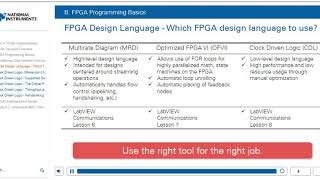
- Design Entry: Utilize Hardware Description Languages (HDLs) like VHDL or Verilog for creating a description of the logical operations.
- Synthesis: Convert HDL code into a gate-level representation compatible with FPGA logic blocks, optimizing for speed, area, and power.
- Implementation: The synthesized design is then placed and routed, determining how logic blocks are configured within the FPGA.
- Simulation and Verification: Before hardware programming, ensure that the design works as intended through simulations.
- Programming the FPGA: After verification, compile the design into a bitstream and program the FPGA accordingly.
- Testing and Debugging: Finally, validate the FPGA's performance with real hardware, using tools for analysis.
The FPGA design flow is significant as it ensures that all aspects of the design and implementation are systematically approached, enabling reliable and efficient digital circuits.
Youtube Videos
Audio Book
Dive deep into the subject with an immersive audiobook experience.
Stage 1: Specification and Requirements Definition
Chapter 1 of 7
🔒 Unlock Audio Chapter
Sign up and enroll to access the full audio experience
Chapter Content
Define the functional requirements and performance goals of the system. This stage involves understanding the problem and creating a detailed specification.
Detailed Explanation
In the first step of the FPGA design flow, the importance of defining the specifications cannot be overstated. This means clearly outlining what you want your design to accomplish. You have to consider aspects like the functionality of the design, how fast it needs to process data, and other performance metrics. It's crucial to have a solid understanding of the problem you're trying to solve before you move forward with the design.
Examples & Analogies
Think of this stage like planning a vacation. Before booking a trip, you need to determine where you want to go, how long you'll stay, what activities you want to do, and your budget. Just as these details help create a great vacation, a well-defined specification ensures the FPGA design meets its intended goals.
Stage 2: Design Entry
Chapter 2 of 7
🔒 Unlock Audio Chapter
Sign up and enroll to access the full audio experience
Chapter Content
In this stage, the design is specified using hardware description languages (HDLs) such as VHDL or Verilog. You can either write the code manually or use a high-level design tool that supports graphical design entry.
Detailed Explanation
During the design entry stage, you'll translate your defined specifications into a format that the FPGA can understand. This is done using hardware description languages (HDLs), which are programming languages specifically for hardware design. You can choose to write the code manually or use software tools that allow for a more visual approach, making it easier for designers to implement complex logic without deep knowledge of the code syntax.
Examples & Analogies
Imagine writing a recipe to make a cake. You need to list ingredients and steps clearly for the cake to turn out well. In FPGA design, coding in HDLs is like writing that recipe; it needs to be precise so that the FPGA knows exactly what to do.
Stage 3: Synthesis
Chapter 3 of 7
🔒 Unlock Audio Chapter
Sign up and enroll to access the full audio experience
Chapter Content
The HDL code is synthesized into a gate-level representation that maps the design onto the FPGA’s programmable logic blocks. This process involves optimizing the design for speed, area, and power consumption.
Detailed Explanation
Synthesis is the phase where the HDL code is transformed from a high-level description into a lower-level representation that can be physically implemented on the FPGA. During synthesis, the design is optimized for several factors: speed (how fast it operates), area (how much space it occupies on the FPGA), and power consumption (how much energy it uses). Effective synthesis is crucial to achieving a functional and efficient design.
Examples & Analogies
Think of synthesis as preparing a dish in a restaurant. Chefs must ensure that a dish not only tastes great but is presented beautifully (area), served quickly (speed), and is cost-effective (power). Just like this balancing act is necessary in culinary arts, synthesis requires optimization in FPGA designs.
Stage 4: Implementation
Chapter 4 of 7
🔒 Unlock Audio Chapter
Sign up and enroll to access the full audio experience
Chapter Content
The synthesized design is placed and routed onto the FPGA fabric. The place-and-route process determines how the logic blocks and routing resources are mapped onto the FPGA.
Detailed Explanation
In the implementation phase, the synthesized design is physically arranged on the FPGA. This involves two key tasks: 'placing' the logic blocks within the FPGA and 'routing' the connections between them. The place-and-route process ensures that the components are arranged efficiently to minimize delays and optimize performance.
Examples & Analogies
Consider arranging furniture in a room. You want to position everything not only for aesthetics but also to allow for smooth traffic flow. Similarly, place-and-route in FPGA design ensures that all components are optimally located for the best performance.
Stage 5: Simulation and Verification
Chapter 5 of 7
🔒 Unlock Audio Chapter
Sign up and enroll to access the full audio experience
Chapter Content
Before programming the FPGA, the design is simulated to ensure it behaves correctly. Simulation tools like ModelSim or Vivado Simulator can be used to check functionality and timing.
Detailed Explanation
Before finalizing the design, it's crucial to test it through simulation. This stage allows designers to run the code in a virtual environment to see how it performs without needing to load it onto the physical FPGA. Verification helps catch errors and ensure that the design meets the specified requirements before deployment. Tools like ModelSim aid in this process by providing insights into timing and functionality.
Examples & Analogies
Visualize a dress rehearsal before a play. Actors practice their lines, and the director checks for any issues before the opening night. Simulation in FPGA design serves the same purpose by allowing complete verification before making the design a reality.
Stage 6: Programming the FPGA
Chapter 6 of 7
🔒 Unlock Audio Chapter
Sign up and enroll to access the full audio experience
Chapter Content
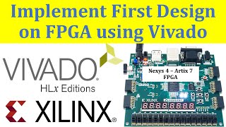
Once verified, the design is compiled and programmed into the FPGA. This can be done using a tool like Xilinx ISE, Vivado, or Intel Quartus.
Detailed Explanation
After successful verification, the next step is to program the FPGA with the synthesized design. This is done by generating a configuration bitstream that allows the FPGA to configure itself according to the design. Software tools like Xilinx ISE or Vivado manage this process efficiently, ensuring that the FPGA is set up to function exactly as intended.
Examples & Analogies
This stage is akin to installing software on a computer. Just as you load software to enable a computer to run applications, you load the design into the FPGA to enable it to perform specific tasks.
Stage 7: Testing and Debugging
Chapter 7 of 7
🔒 Unlock Audio Chapter
Sign up and enroll to access the full audio experience
Chapter Content
The final step is to test the FPGA on the actual hardware. Tools like in-circuit debuggers and logic analyzers are used to validate the system’s performance and behavior.
Detailed Explanation
Once the FPGA is programmed, the final step involves testing it in real hardware. This is crucial for ensuring that the design works as expected in its operational environment. Tools such as in-circuit debuggers and logic analyzers assist in identifying any issues and validating performance, making sure everything operates smoothly.
Examples & Analogies
Consider launching a new product. Before it hits the market, companies conduct thorough testing to catch any flaws that need addressing. Similarly, this testing phase ensures that the FPGA performs correctly and reliably in real-world applications.
Key Concepts
-
Specification: The foundation for design; defines what the FPGA must accomplish.
-
Design Entry: Utilizing HDLs to represent logic; crucial for clarity.
-
Synthesis: Transforming HDL into gate-level logic; optimizing for area and performance.
-
Implementation: Mapping logical representation onto actual FPGA architecture.
-
Simulation: Verifying the design's correctness before physical programming.
Examples & Applications
Creating a VHDL description of a counter for testing.
Using simulation tools like ModelSim to check the design functionality of an FPGA project.
Memory Aids
Interactive tools to help you remember key concepts
Rhymes
In FPGA design, start with specs so fine, then enter data, your path will align.
Stories
Imagine a wizard creating a magical object; he first defines what it should do (specification), then he sketches his plans (design entry), and finally turns it into something real (synthesis).
Memory Tools
Remember the 'SIPS' for FPGA design flow: Specs, Input, Process, Simulate.
Acronyms
The 'DIPSP' acronym for FPGA requires
Design Input
Synthesis
Placement.
Flash Cards
Glossary
- Spec
A detailed outline of the functional and performance requirements of the FPGA design.
- HDL
Hardware Description Language used to describe the structure and behavior of electronic systems.
- Synthesis
The process of converting HDL code into a gate-level representation.
- Implementation
The placing and routing of the synthesized design onto the FPGA fabric.
- Simulation
The procedure of checking the functionality of a design through computational models before physical deployment.
Reference links
Supplementary resources to enhance your learning experience.