
Implementation
Interactive Audio Lesson
Listen to a student-teacher conversation explaining the topic in a relatable way.
Overview of the Implementation Process
🔒 Unlock Audio Lesson
Sign up and enroll to listen to this audio lesson

Today, we are going to discuss the implementation stage of FPGA design. This is where our synthesized designs are actually placed and routed on the FPGA fabric. Can anyone tell me what they think placement and routing involve?

Placement is like deciding where to put every piece of furniture in a room, right?
Exactly! Placement is about deciding where each logic block will go on the FPGA. Now, can someone tell me what routing means?

Isn't routing about connecting these blocks, like running wires between them?
Correct! Routing connects the logic blocks through programmable interconnects. Remember the mnemonic 'PR' - Placement & Routing!

What happens if the placement isn't efficient?
Good question! Inefficient placement can lead to longer signal paths and timing issues, which we want to avoid. Let's move on to discuss the tools we use for this process.
Tools Used for Implementation
🔒 Unlock Audio Lesson
Sign up and enroll to listen to this audio lesson

Now let’s talk about the tools we use for implementation. Can anyone name a tool commonly used for this process?

I've heard of Xilinx Vivado.
That's right! Xilinx Vivado is indeed a popular tool. What about another one?
Intel Quartus?
Perfect! Both tools assist in the placement and routing of designs. Remember their names for your projects! Can someone summarize what we learned about importance of these tools?
They help us optimize designs for speed and resource use!
Exactly! Great job! Let's dive deeper into what happens after implementation.
Post-Implementation Verification
🔒 Unlock Audio Lesson
Sign up and enroll to listen to this audio lesson
After implementation, testing is critical. Can anyone think of why we need to test the design after placing and routing?
To make sure it works as intended?
Yes! We want to verify functionality and timing. We often use simulation tools to ensure everything behaves correctly. Can anyone name such a tool?
ModelSim!
Great! ModelSim is one option among others. Remember, testing helps us catch issues early. Let’s summarize what we discussed today.
We learned about placement and routing, tools like Vivado and Quartus, and the importance of testing!
Exactly! Well done, everyone!
Introduction & Overview
Read summaries of the section's main ideas at different levels of detail.
Quick Overview
Standard
The implementation stage is a crucial part of FPGA design flow, where the synthesized code is physically arranged and connected on the FPGA. This section details the steps involved in the implementation process, the tools used, and its significance in ensuring that designs meet timing and resource requirements.
Detailed
Detailed Summary of Implementation
The implementation stage in FPGA design is a key step where the synthesized design—produced from high-level description languages—is mapped onto the FPGA fabric. It consists of two main processes: placement and routing.
- Placement: This involves determining where the logic blocks and other resources will be physically located on the FPGA. The placement should ensure efficient use of resources while meeting timing constraints.
- Routing: This phase connects the logic blocks through the programmable interconnects according to the design specifications. Proper routing is essential to ensure signal integrity and minimize propagation delays.
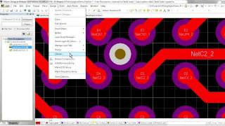
Tools like Xilinx Vivado or Intel Quartus handle these processes, optimizing the layout for various factors, including area, power, and speed. Successful implementation is crucial for verifying that the design will function correctly when programmed into the FPGA, laying the groundwork for subsequent testing and debugging phases.
Youtube Videos
Audio Book
Dive deep into the subject with an immersive audiobook experience.
Overview of Implementation
Chapter 1 of 2
🔒 Unlock Audio Chapter
Sign up and enroll to access the full audio experience
Chapter Content
The synthesized design is placed and routed onto the FPGA fabric. The place-and-route process determines how the logic blocks and routing resources are mapped onto the FPGA.
Detailed Explanation
In this stage of the FPGA design flow, after the design has been synthesized, it must be organized for the FPGA hardware. This is called the 'place-and-route' process. Basically, this means that the synthesized design needs to be positioned correctly on the FPGA's architecture (which consists of various logic blocks) and connected properly through the programmable routing resources. The goal is to optimize the layout to ensure efficiency in speed and resource use. Proper placement means minimizing the distance signals need to travel, which can improve the overall performance of the FPGA.
Examples & Analogies
Think of the place-and-route process like arranging furniture in a room. You want to place each piece of furniture (logic blocks) in a way that they fit well and allow for easy movement (signal flow) throughout the room. If furniture is too far apart or obstructs pathways, it can lead to inefficiencies, just like a poorly arranged FPGA design may slow down the processing speed of the digital circuits.
Key Steps in Place-and-Route Process
Chapter 2 of 2
🔒 Unlock Audio Chapter
Sign up and enroll to access the full audio experience
Chapter Content
The place-and-route process involves determining the locations of logic blocks, optimizing routing paths, and ensuring that all timing constraints are met.
Detailed Explanation
The place-and-route process involves several key activities: first, the logic blocks (which perform the computational tasks) need to be placed in optimal locations on the FPGA. Next, the interconnections (or routing paths) between these blocks must be optimized to reduce delay and ensure signal integrity. Finally, designers need to check that all timing constraints are adhered to so that data flows correctly without causing errors. Timing constraints ensure that all signals are synchronized and processed at the right moments, which is crucial for the reliable operation of digital systems.
Examples & Analogies
Imagine you're setting up a relay race. Each runner represents a logic block, and the path between them represents the routing. You want each runner to be positioned so they can pass the baton without delay and in the correct order. If one runner is too far away, or if they run at different speeds, the relay may be inefficient or even fail. Similarly, in the FPGA place-and-route process, proper positioning and routing paths lead to a more efficient design.
Key Concepts
-
Implementation: The process where the design is physically mapped onto an FPGA via placement and routing.
-
Placement: Determining physical locations for logic blocks to optimize resource usage.
-
Routing: Connecting the logic blocks through interconnects to achieve the desired functionality.
-
Verification: Testing the implemented design to ensure it works correctly.
Examples & Applications
A digital circuit designed to perform a specific function, such as an adder, shows how placement and routing are used to realize the design on an FPGA.
Using Xilinx Vivado, a designer routes the paths between several logic blocks ensuring that the timing constraints are met for an efficient design.
Memory Aids
Interactive tools to help you remember key concepts
Rhymes
To place the blocks in the right spot, routing connections hits the right spot.
Stories
Imagine an architect laying out a building (placement) and then connecting the paths (routing) so everyone can find their way.
Memory Tools
Remember 'PR' for Placement and Routing in FPGA design.
Acronyms
PR
Placement & Routing for FPGA Design Flow.
Flash Cards
Glossary
- Implementation
The process of placing and routing a design onto an FPGA's configuration fabric.
- Placement
The stage of implementation where logic blocks are assigned specific physical locations on an FPGA.
- Routing
The process of defining how logic blocks are connected via programmable interconnects within the FPGA.
- Synthesis
The process of converting high-level design code (such as VHDL or Verilog) into a gate-level representation for implementation.
- Simulation
The method of verifying the design's functionality and timing before programming the FPGA.
Reference links
Supplementary resources to enhance your learning experience.